
Network Card User Manual


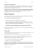
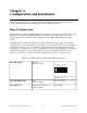


Table Of Contents
- PC-DIO-24 User Manual
- Contents
- About This Manual
- Chapter 1 Introduction
- Chapter 2 Configuration and Installation
- Chapter 3 Theory of Operation
- Chapter 4 Register-Level Programming
- Appendix A Specifications
- Appendix B I/O Connector
- Appendix C OKI 82C55A Data Sheet*
- Appendix D Customer Communication
- Glossary
- Index
- Figures
- Figure 1-1. The Relationship between the Programming Environment, NI-DAQ, and Your Hardware
- Figure 2-1. PC-DIO-24 Parts Locator Diagram
- Figure 2-2. Example Base I/O Address Switch Settings
- Figure 2-3. Jumper Settings–PC6, PC4, PC2, and N/C
- Figure 2-4. Interrupt Jumper Setting for IRQ5 (Factory Setting)
- Figure 2-5. Digital I/O Connector Pin Assignments
- Figure 3-1. PC-DIO-24 Block Diagram
- Figure 4-1. Control-Word Formats
- Figure B-1. PC-DIO-24 I/O Connector
- Tables
- Table 2-1. PC-DIO-24 Factory-Set Jumper and Switch Settings
- Table 2-2. Port C Signal Assignments
- Table 4-1. PC-DIO-24 Address Map
- Table 4-2. Port C Set/Reset Control Words
- Table 4-3. Mode 0 I/O Configurations
- Table 4-4. Interrupt Enable Signals for All Mode Combinations
- Table A-1. Maximum Average Transfer Rates for the PC-DIO-24

Chapter 2 Configuration and Installation
© National Instruments Corporation 2-3 PC-DIO-24 User Manual
U2 DIP switches, press the side marked OFF to select a binary value of 1 for the corresponding
address bit. Press the other side of the switch to select a binary value of 0 for the corresponding
address bit. Figure 2-2 shows two possible switch settings. The black side indicates the side that
is pushed down.
O
F
F
12345678
O
N
U2
A9
A8
A7
A6
A5
A4
A3
A2
A. Switches Set to Default Setting (Base I/O Address Hex 210)
O
F
F
12345678
O
N
U2
A9
A8
A7
A6
A5
A4
A3
A2
B. Switches Set to Base I/O Address Hex 278
Figure 2-2. Example Base I/O Address Switch Settings