
NI PCI-6110/6111 User Manual

Chapter 4 Connecting Signals
NI PCI-6110/6111 User Manual 4-6 ni.com
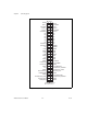
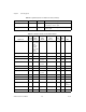
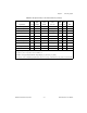
GPCTR0_OUT DGND Output Counter 0 Output—This output is from the
general-purpose counter 0 output.
FREQ_OUT DGND Output Frequency Output—This output is from the frequency
generator output.
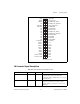
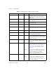
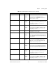
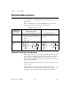
Table 4-3. I/O Signal Summary for the NI PCI-6110/6111
Signal Name
Signal
Type and
Direction
Impedance
Input/
Output
Protection
(Volts)
On/Off
Source
(mA at V)
Sink
(mA at V)
Rise
Time
(ns)
Bias
ACH<0..3>+ AI 1MΩ
in parallel
with
100 pF
1
1MΩ
in parallel
with
10 pF
2
42 V — — — —
ACH<0..3>– AI 10 nF 42 V — — — ±200 pA
ACH<0..3>GND AI — — — — — —
DAC0OUT AO 50 Ω Short-circuit
to ground
5 at 10 5 at –10 300
V/µs
—
DAC1OUT AO 50 Ω Short-circuit
to ground
5 at 10 5 at –10 300
V/µs
—
AOGND AO — — — — — —
DGND DO — — — — — —
VCC DO 0.1 Ω Short-circuit
to ground
1 A — — —
DIO<0..7> DIO — V
cc
+0.5 13 at (V
cc
–0.4) 24 at0.4 1.1 50 kΩ pu
SCANCLK DO — — 3.5 at (V
cc
–0.4) 5 at 0.4 1.5 50 kΩ pu
EXTSTROBE* DO — — 3.5 at (V
cc
–0.4) 5 at 0.4 1.5 50 kΩ pu
PFI0/TRIG1 AI/DIO 10 kΩ ±35 V
cc
+0.5 3.5 at (V
cc
–0.4) 5 at 0.4 1.5 9kΩ pu
and
10 kΩ pd
PFI1/TRIG2 DIO — V
cc
+0.5 3.5 at (V
cc
–0.4) 5 at 0.4 1.5 50 kΩ pu
PFI2/CONVERT* DIO — V
cc
+0.5 3.5 at (V
cc
–0.4) 5 at 0.4 1.5 50 kΩ pu
Table 4-2. Signal Descriptions for I/O Connector Pins (Continued)
Signal Name Reference Direction Description