
NI PCI-6110/6111 User Manual

Chapter 4 Connecting Signals
NI PCI-6110/6111 User Manual 4-4 ni.com
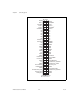
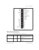
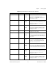
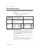
ACH<0..3>– ACH<0..3>GND Input Analog Input Channels 0 through 3 (–)—These pins are
routed to the (–) terminal of the respective channel
amplifier. ACH<2..3>– signals are no connects on the
NI PCI-6111.
DAC0OUT AOGND Output Analog Channel 0 Output—This pin supplies the voltage
output of AO channel 0.
DAC1OUT AOGND Output Analog Channel 1 Output—This pin supplies the voltage
output of AO channel 1.
AOGND — — Analog Output Ground—The AO voltages are referenced
to this node.
DGND — — Digital Ground—This pin supplies the reference for the
digital signals at the I/O connector as well as the +5 VDC
supply.
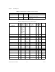
DIO<0..7> DGND Input or
Output
Digital I/O signals—DIO6 and 7 can control the up/down
signal of general-purpose counters 0 and 1, respectively.
+5 V DGND Output +5 VDC Source—These pins are fused for up to 1 A of
+5 V supply. The fuse is self-resetting.
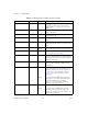
SCANCLK DGND Output Scan Clock—This pin pulses once for each A/D
conversion when enabled. The low-to-high edge indicates
when the input signal can be removed from the input or
switched to another signal.
EXTSTROBE* DGND Output External Strobe—This output can be toggled under
software control to latch signals or trigger events on
external devices.
PFI0/TRIG1 DGND Input
Output
PFI0/Trigger 1—As an input, this is either a PFI or the
source for the hardware analog trigger. PFI signals are
explained in the Timing Connections section. Refer to
the Analog Trigger section of Chapter 3, Hardware
Overview, for more information about the hardware
analog trigger.
As an output, this is the TRIG1 signal. In posttrigger
DAQ sequences, a low-to-high transition indicates the
initiation of the DAQ sequence. In pretrigger
applications, a low-to-high transition indicates the
initiation of the pretrigger conversions.
PFI1/TRIG2 DGND Input
Output
PFI1/Trigger 2—As an input, this is a PFI.
As an output, this is the TRIG2 signal. In pretrigger
applications, a low-to-high transition indicates the
initiation of the posttrigger conversions. TRIG2 is not
used in posttrigger applications.
Table 4-2. Signal Descriptions for I/O Connector Pins (Continued)
Signal Name Reference Direction Description