
Digital Input/Output (I/O) Device User Guide and Specifications

NI 6509 User Guide and Specifications 20 ni.com
Power-on state ........................................Inputs high-Z (default),
user-selectable input,
output 1 or 0
Data transfers..........................................Interrupts, programmed I/O
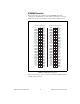
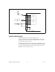
I/O connector ..........................................100-pin female 0.050 series SCSI
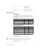
Digital Logic Levels
Input Signals
The maximum input logic high and output logic high voltages assume a
Vcc supply voltage of 5.0 V. Given a Vcc supply voltage of 5.0 V, the
absolute maximum voltage rating for each I/O line is –0.5 V to 5.5 V with
respect to GND.
Output Signals (Vcc = 5 V)
The total current sinking/sourcing from one port cannot exceed 100 mA.
+5V power available at
I/O connector (pins 49 and 99) ...............+4.65 to +5.25 V
Note The I/O connector power has a fuse for overcurrent protection. This fuse is not
customer replaceable. If the fuse is blown, return the device to NI for repair.
Programmable power-up states
response time ..........................................400 ms
Level Min Max
Input voltage (V
I
) 0 V Vcc
Input logic low voltage (V
IL
) — 0.8 V
Input logic high voltage (V
IH
) 2 V —
Level Min Max
High-level output current (I
OH
) — –24 mA
Low-level output current (I
OL
) — 24 mA
Output voltage (V
O
) 0 Vcc
Output low voltage (V
OL
), at 24 mA — 0.55 V
Output high voltage (V
OH
), at –24 mA 3.7 V —