
- National Semiconductor High-Performance Microcontrollers Specification Sheet

20 MHz
AC Electrical Characteristics
(See Notes 1 and 4 and
Figures 1
thru
5
). V
CC
e
5V
g
5%*,T
A
eb
55
§
Cto
a
125
§
C for HPC167064 and V
CC
e
5V
g
10%,
T
A
e
0
§
Cto
a
70
§
C for HPC467064
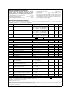
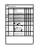
Symbol and Formula Parameter Min Max Units Notes
f
C
CKI Operating Frequency 2 20 MHz
t
C1
e
1/f
C
CKI Clock Period 50 500 ns
t
CKIH
CKI High Time 22.5 ns
t
CKIL
CKI Low Time 22.5 ns
t
C
e
2/f
C
CPU Timing Cycle 100 ns
t
WAIT
e
t
C
CPU Wait State Period 100 ns
t
DC1C2R
Delay of CK2 Rising Edge after CKI Falling Edge 0 55 ns (Note 2)
t
DC1C2F
Delay of CK2 Falling Edge after CKI Falling Edge 0 55 ns (Note 2)
f
U
e
f
C
/8 External UART Clock Input Frequency 2.5** MHz
f
MW
External MICROWIRE/PLUS Clock Input Frequency 1.25 MHz
f
XIN
e
f
C
/22 External Timer Input Frequency 0.91 MHz
t
XIN
e
t
C
Pulse Width for Timer Inputs 100 ns
t
UWS
MICROWIRE Setup TimeÐMaster 100
ns
MICROWIRE Setup TimeÐSlave 20
t
UWH
MICROWIRE Hold TimeÐMaster 20
ns
MICROWIRE Hold TimeÐSlave 50
t
UWV
MICROWIRE Output Valid TimeÐMaster 50
ns
MICROWIRE Output Valid TimeÐSlave 150
t
SALE
e
*/4 t
C
a
40 HLD Falling Edge before ALE Rising Edge 115 ns
t
HWP
e
t
C
a
10 HLD Pulse Width 110 ns
t
HAE
e
t
C
a
100 HLDA Falling Edge after HLD Falling Edge 200 ns (Note 3)
t
HAD
e
*/4 t
C
a
85 HLDA Rising Edge after HLD Rising Edge 160 ns
t
BF
e
(/2 t
C
a
66 Bus Float after HLDA Falling Edge 116 ns (Note 5)
t
BE
e
(/2 t
C
a
66 Bus Enable after HLDA
Rising Edge 116 ns (Note 5)
t
UAS
Address Setup Time to Falling Edge of URD 10 ns
t
UAH
Address Hold Time from Rising Edge of URD 10 ns
t
RPW
URD Pulse Width 100 ns
t
OE
URD Falling Edge to Output Data Valid 0 60 ns
t
OD
Rising Edge of URD to Output Data Invalid 5 45 ns (Note 6)
t
DRDY
RDRDY Delay from Rising Edge of URD 70 ns
t
WDW
UWR Pulse Width 40 ns
t
UDS
Input Data Valid before Rising Edge of UWR 10 ns
t
UDH
(HPC467064) Input Data Hold after Rising Edge of UWR 20 ns
t
UDH
(HPC167064) 25* ns
t
A
WRRDY Delay from Rising Edge of UWR 70 ns
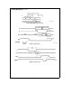
ClocksTimersMicrowire/PlusExternal HoldUPI Timing
*See NORMAL RUNNING MODE.
**This maximum frequency is attainable provided that this external baud clock has a duty cycle such that the high period includes two (2) falling edges of the CK2
clock.
Note: C
L
e
40 pF.
Note 1: These AC Characteristics are guaranteed with external clock drive on CKI having 50% duty cycle and with less than 15 pF load on CKO with rise and fall
times (t
CKIR
and t
CKIL
) on CKI input less than 2.5 ns.
Note 2: Do not design with this parameter unless CKI is driven with an active signal. When using a passive crystal circuit, its stability is not guaranteed if either CKI
or CKO is connected to any external logic other than the passive components of the crystal circuit.
Note 3: t
HAE
is spec’d for case with HLD falling edge occurring at the latest time can be accepted during the present CPU cycle being executed. If HLD falling edge
occurs later, t
HAE
may be as long as (3t
C
a
4WS
a
72t
C
a
100) depending on the following CPU instruction cycles, its wait states and ready input.
Note 4: WS
e
t
WAIT
c
(number of pre-programmed wait states). Minimum and maximum values are calculated at maximum operating frequency, t
c
e
20.00 MHz,
with one wait state programmed.
Note 5: Due to emulation restrictionsÐactual limits will be better.
Note 6: Due to tester limitationsÐactual limits will be better.
3