
- National Semiconductor High-Performance Microcontrollers Specification Sheet


Pin Descriptions
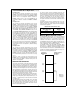
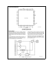
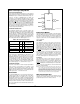
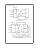
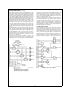
The HPC167064 is available only in 68-pin LDCC package.
I/O PORTS
Port A is a 16-bit bidirectional I/O port with a data direction
register to enable each separate pin to be individually de-
fined as an input or output. When accessing external memo-
ry, port A is used as the multiplexed address/data bus.
Port B is a 16-bit port with 12 bits of bidirectional I/O similar
in structure to Port A. Pins B10, B11, B12 and B15 are gen-
eral purpose outputs only in this mode. Port B may also be
configured via a 16-bit function register BFUN to individually
allow each pin to have an alternate function.
B0: TDX UART Data Output
B1:
B2: CKX UART Clock (Input or Output)
B3: T2IO Timer2 I/O Pin
B4: T3IO Timer3 I/O Pin
B5: SO MICROWIRE/PLUS Output
B6: SK MICROWIRE/PLUS Clock (Input or Output)
B7: HLDA
Hold Acknowledge Output
B8: TS0 Timer Synchronous Output
B9: TS1 Timer Synchronous Output
B10: UA0 Address 0 Input for UPI Mode
B11: WRRDY
Write Ready Output for UPI Mode
B12:
B13: TS2 Timer Synchronous Output
B14: TS3 Timer Synchronous Output
B15: RDRDY
Read Ready Output for UPI Mode
When accessing external memory, four bits of port B are
used as follows:
B10: ALE Address Latch Enable Output
B11: WR
Write Output
B12: HBE
High Byte Enable Output/Input
(sampled at reset)
B15: RD
Read Output
Port I is an 8-bit input port that can be read as general
purpose inputs and is also used for the following functions:
I0:
I1: NMI Nonmaskable Interrupt Input
I2: INT2 Maskable Interrupt/Input Capture/URD
I3: INT3 Maskable Interrupt/Input Capture/UWR
I4: INT4 Maskable Interrupt/Input Capture
I5: SI MICROWIRE/PLUS Data Input
I6: RDX UART Data Input
I7:
Port D is an 8-bit input port that can be used as general
purpose digital inputs.
Port P is a 4-bit output port that can be used as general
purpose data, or selected to be controlled by timers 4
through 7 in order to generate frequency, duty cycle and
pulse width modulated outputs.
POWER SUPPLY PINS
V
CC1
and
V
CC2
Positive Power Supply
GND Ground for On-Chip Logic
DGND Ground for Output Buffers
Note: There are two electrically connected V
CC
pins on the chip, GND and
DGND are electrically isolated. Both V
CC
pins and both ground pins
must be used.
CLOCK PINS
CKI The Chip System Clock Input
CKO The Chip System Clock Output (inversion of CKI)
Pins CKI and CKO are usually connected across an external
crystal.
CK2 Clock Output (CKI divided by 2)
OTHER PINS
WO
This is an active low open drain output that sig-
nals an illegal situation has been detected by the
WATCHDOG logic.
ST1 Bus Cycle Status Output: indicates first opcode
fetch.
ST2 Bus Cycle Status Output: indicates machine
states (skip, interrupt and first instruction cycle).
RESET
is an active low input that forces the chip to re-
start and sets the ports in a TRI-STATE mode.
RDY/HLD
has two uses, selected by a software bit. It’s ei-
ther an input to extend the bus cycle for slower
memories, or a HOLD request input to put the
bus in a high impedance state for DMA purpos-
es.
NC (no connection) do not connect anything to this
pin.
EXM Has two uses. External memory enable (active
high) which disables internal EPROM and maps
it to external memory, and is V
PP
during EPROM
mode.
EI External interrupt with vector address
FFF1:FFF0. (Rising/falling edge or high/low lev-
el sensitive). Alternately can be configured as
4th input capture.
EXUI
External interrupt which is internally OR’ed with
the UART interrupt with vector address
FFF3:FFF2 (Active Low).
12