
- National Semiconductor Memory Interface Circuits Specification Sheet

TL/F/5012– 8
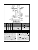
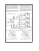
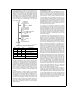
FIGURE 7a. Typical Power Dissipation for DP84240 at
V
CC
e
5.5V (All 8 drivers switching simultaneously)
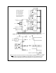
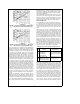
TL/F/5012– 9
FIGURE 7b. Typical Power Dissipation for DP84244 at
V
CC
e
5.5V (All 8 drivers switching simultaneously)
The output stages of the DP84240 and the DP84244, al-
though well matched, are relatively low impedance. Output
impedance is under 10X. Some DRAM arrays will require
the addition of damping resistors in series with the outputs
of the drivers. These damping resistors are used to minimize
undershoot which may have a harmful effect on the DRAMs
if allowed to become large. This undershoot is caused by
the high transient currents from the drivers necessary to
drive the capacitive loads. These high currents pass through
a distributed inductive/capacitive circuit created by the
board traces and the DRAM load, causing the undershoot.
The damping resistor has specifically not been placed on-
chip because its value is dependent on the DRAM array size
and board layout. In fact, address lines will quite often re-
quire a different resistor value from the DRAM control lines.
The resistor must be tuned for a particular board layout
since too high a resistor will produce an excessively slow
edge and too low a resistor will not remove the udershoot.
Values for damping resistors may vary from 15X to 150X,
depending on the application. Placing any value of damping
resistor on-chip, other than a value less than the minimum,
severely restricts the application of these high performance
circuits.
Another key advantage of both the DP84240 and the
DP84244 is their low input capacitance. Previous address
buffer/drivers (such as the DM74S240/244) have high input
capacitance. Fast edges at the inputs of these drivers be-
come slower and distorted due to this dynamic input capaci-
tance. This problem must be factored as an additional delay
through these driversÐa delay not shown by the data sheet
specifications. Additionally, the problem becomes increas-
ingly severe as multiple driver inputs are used in parallel for
bus expansion applications.
Both the DP84240 and the DP84244 are designed to signifi-
cantly reduce both static and dynamic input capacitance.
When these devices are driven with standard logic circuits,
no appreciable overhead delay need be added to the basic
device delay specifications due to input pulse distortion.
ERROR CORRECTION
The determination of whether a DRAM system requires er-
ror correction must be resolved early in the system design.
A positive answer to this question may have far-reaching
impact on board development time and component cost. It
is clear, however, that such a decision cannot be taken
lightly.
The type and origin of errors in DRAM systems are many
and can result from a number of sources (Table III). Current
estimates of soft error rates due to alpha particles in 64k
RAMs indicate some hope that these error rates will be simi-
lar or possibly better than those found in 16k DRAMsÐbut
the facts are still somewhat unclear. However, it is clear that
the use of 256k DRAMs and the introduction in the near
future of 1 Mbit DRAMs with even smaller memory cells and
greater chip densities will place a significant challenge on
DRAM chip designers to keep these rates down. It is be-
lieved by some that error correction may become mandato-
ry in future DRAM system designs. Currently, the decision to
add error correction is not so straightforward. It depends on
many factors, not the least of which is the end user’s per-
ception of its value to system uptime and reliability.
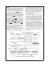
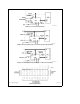
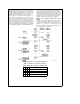
TABLE III. The Sources and Types of Memory Errors
Error
Sources System Action
Type
#
Alpha Particles Temporary system errorÐ
may be overwritten with a
Soft
#
System Noise
low probability of repetition
#
Chip Patterns
#
Power Glitches
#
Stuck Memory Bit Permanent failureÐmay
act as logic 1 or 0
Hard
#
Memory Chip Interface
#
Interface Circuit Failure
Generally, error correction will always be found in highly reli-
able systems during DRAMs, such as process control equip-
ment, banking terminals, and military systems where high
data integrity and minimum downtime are priorities. Howev-
er, the importance of error correction has grown substantial-
ly, to the point that it is now used as selling feature in the
vast majority of large memory-based systems. In fact, some
major computer houses have adopted quidelines for use by
their designers in the development of DRAM arrays. A
somewhat common set has been foundÐif the memory ar-
ray is on the order of (/4 million bytes, then word parity
should be used. This permits the detection of single bit er-
rors but does not allow error correction. When the total
memory approaches (/2 million bytes, then double bit error
detection and single bit error correction should be added.
The decision to add error correction to a system is costly,
both in memory overhead and control hardware. Table IV
6