
- National Semiconductor Memory Interface Circuits Specification Sheet
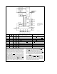
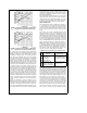
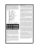

Drams may be 16k, 64k or 256k
For 4 banks, can drive 16 data
bits
a
6 check bits for ECC.
For 2 banks, can drive 32 data
bits
a
7 check bits for ECC.
For 1 bank, can drive 64 data
bits
a
8 check bits for ECC.
*These outputs may need damping
resistors to prevent overshoot,
undershoot at memories.
TL/F/5012– 2
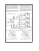
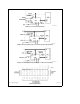
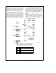
FIGURE 2. Typical Application of DP8409A Using External Control and Refresh in Modes 0 and 4
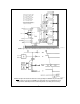
TL/F/5012– 3
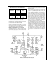
FIGURE 3. This figure demonstrates the automatic accessing capability of the DP8409A. Only one strobing edge,
RASIN
, is required for generation of all DRAM access timing signals. This is accomplished with on-chip
delay generators, eliminating the need for external delay lines. No access timing clock is necessary.
3