
- National Semiconductor Memory Interface Circuits Specification Sheet

Indicates that there is a 3
kX pull-up resistor on
these outputs when they
are disabled.
TL/F/5012–1
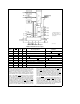
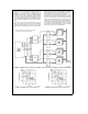
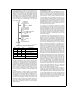
FIGURE 1. DP8409A Block Diagram
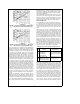
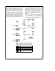
TABLE II. DP8409A Mode Select Options
Mode
(RFSH
)
M1 M0 Mode of Operation Conditions
M2
0 0 0 0 Externally Controlled Refresh RF I/O
e
EOC
1 0 0 1 Auto RefreshÐForced RF I/O
e
Refresh Request (RFRQ)
2 0 1 0 Internal Auto Burst Refresh RF I/O
e
EOC
3a 0 1 1 All RAS Auto Write RF I/O
e
EOC
3b 0 1 1 Externally Controlled All RAS Access All RAS Active
4 1 0 0 Externally Controlled Access
5 1 0 1 Auto Access, Slow t
RAH
, Hidden Refresh
6 1 1 0 Auto Access, Fast t
RAH
7 1 1 1 Set End of Count
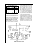
Modes 0, 3b, and 4 provide full control of access and re-
fresh for systems with external memory controllers or for
special purpose applications. Here all timing can be directly
controlled by the external system as shown in
Figure 2
.
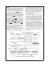
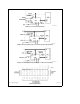
Modes 1, 5 and 6 provide on-chip automatic access se-
quencing with hidden refresh capability. A graphic example
of the automatic access modes of the DP8409A is shown in
Figure 3
. All DRAM access timing and control is generated
from one input strobe, RASIN
; no external clock is required.
On-chip delays insure proper address and control sequenc-
ing once the valid parallel address is presented to the fall-
through input latches of the DP8409A. When the RASIN
transitions high-to-low, the decoded RAS output transitions
low, strobing the row address into the DRAM array. An on-
chip delay automatically generates a guaranteed selectable
(mode 5 or 6) row address hold time. At this point, the
DP8409A switches the address outputs from the row latch
to the column latch. Then another on-chip delay generates
a guaranteed column address set-up time before CAS
,so
that the CAS
output automatically strobes the column ad-
dress into the DRAM array. Read or write cycles are con-
trolled by the system through independent control of the WE
buffer that is provided on-chip to minimize delay skewing.
The automatic access mode makes the dynamic RAM ap-
pear static with respect to access timing. In this mode, only
one signal, RASIN
, is needed after valid parallel addresses
are presented to the DP8409A to initiate proper access se-
quencing. Access timing (RASIN
to CAS), with full output
loading of 88 DRAMs in the auto access mode, is deter-
mined by the dash number given on the DP8409A data
sheet. All performance characteristics are specified over the
full operating temperature and supply ranges.
2