
user manual
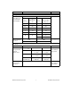
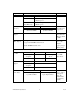
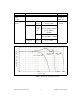
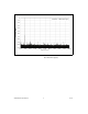
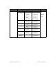
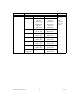
Table Of Contents
- NI PXI/PCI-5124 Specifications
- Contents
- Vertical
- Analog Input (Channel 0 and Channel 1)
- Figure 1. NI 5124 Frequency Response (Typical)
- Figure 2. NI 5124 Dynamic Performance, 50 W , 1 Vpk-pk Range, 262,144 Point FFT (Typical)
- Figure 3. Representation of NI 5124 Spectral Noise Density on 0.2 V Range, Noise Filter Enabled, 1 MW Input Impedance
- Figure 4. Representation of NI 5124 Spectral Noise Density on 0.2 V Range, Full Bandwidth, 50 W Input Impedance
- Analog Input (Channel 0 and Channel 1)
- Horizontal
- Trigger
- PFI 0 and PFI 1 (Programmable Function Interface, AUX Front Panel Connector)
- TClk Specifications
- Waveform Specifications
- Calibration
- Power
- Software
- Environment
- Safety, Electromagnetic Compatibility, and CE Compliance
- Physical
- Where to Go for Support
© National Instruments Corporation 3 NI PXI/PCI-5124 Specifications
Voltage Levels
Full Scale (FS)
Input Range and
Programmable
Vertical Offset
50 Ω 1MΩ —
Range
(V
pk-pk
)
Vertical
Offset Range
(V)
Range
(V
pk-pk
)
Vertical Offset
Range (V)
0.2 ±0.1 0.2 ±0.1
0.4 ±0.2 0.4 ±0.2
1 ±0.5 1 ±0.5
2 ±1 2 ±1
4 ±2 4 ±2
10 0 10 ±5
20 0
Maximum Input
Overload
50 Ω 1MΩ —
7V
rms
with |Peaks| ≤10 V |Peaks| ≤42 V
Accuracy
Resolution 12 bits —
DC Accuracy
(Programmable
Vertical
Offset = 0 V)
Range (V
pk-pk
) NI PXI-5124 NI PCI-5124 Within ±5 °C of
self-calibration
temperature
0.2 and 0.4 ±(0.65% of Input
+ 1.3 mV)
±(0.65% of Input
+ 1.8 mV)
1 and 2 ±(0.65% of Input
+ 1.5 mV)
±(0.65% of Input
+ 2.1 mV)
4, 10, and
20 (1 MΩ only)
±(0.65% of Input
+ 10.0 mV)
±(0.65% of Input
+ 10.0 mV)
Programmable
Vertical Offset
Accuracy
±0.4% of offset setting Within ±5 °C of
self-calibration
temperature
Specification Val ue Comments