
user manual
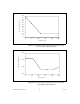

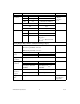
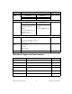
Table Of Contents
- NI PXI/PCI-5124 Specifications
- Contents
- Vertical
- Analog Input (Channel 0 and Channel 1)
- Figure 1. NI 5124 Frequency Response (Typical)
- Figure 2. NI 5124 Dynamic Performance, 50 W , 1 Vpk-pk Range, 262,144 Point FFT (Typical)
- Figure 3. Representation of NI 5124 Spectral Noise Density on 0.2 V Range, Noise Filter Enabled, 1 MW Input Impedance
- Figure 4. Representation of NI 5124 Spectral Noise Density on 0.2 V Range, Full Bandwidth, 50 W Input Impedance
- Analog Input (Channel 0 and Channel 1)
- Horizontal
- Trigger
- PFI 0 and PFI 1 (Programmable Function Interface, AUX Front Panel Connector)
- TClk Specifications
- Waveform Specifications
- Calibration
- Power
- Software
- Environment
- Safety, Electromagnetic Compatibility, and CE Compliance
- Physical
- Where to Go for Support

NI PXI/PCI-5124 Specifications 18 ni.com
Time
Resolution
TDC Onboard Clock External Clock TDC = Time
to Digital
Conversion
Circuit
On 50 ps N/A
Off 5ns External Clock Period
Rearm Time TDC Rearm Time Holdoff set to 0
On 10 μs
Off 2 μs
Holdoff TDC Onboard Clock External Clock —
On 10 μs to 85.899 s N/A
Off 2 μs to 85.899 s 200 × (External Clock
Period) to
(2
32
– 1) × (External Clock
Period)
Analog Trigger (Edge, Window, and Hysteresis Trigger Types)
Sources CH 0 (front panel BNC connector)
CH 1 (front panel BNC connector)
TRIG (front panel BNC connector)
—
Trigger Level
Range
CH 0, CH 1 TRIG (External Trigger) —
100% FS ±5 V
Trigger Level
Resolution
10 bits (1 in 1,024) —
Edge Trigger
Sensitivity
CH 0, CH 1 TRIG (External Trigger) —
3.5% FS up to 50 MHz,
increasing to 10% FS at
150 MHz
0.25 V
pk-pk
up to 100 MHz,
increasing to 1 V
pk-pk
at
200 MHz
Level
Accuracy,
Typical
CH 0, CH 1 TRIG (External Trigger) —
±4.7% FS up to 10 MHz ±0.35 V up to 10 MHz
Trigger
Jitter
≤80 ps rms Within ±5 °C of
self-calibration
temperature
Specification Val ue Comments