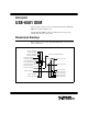
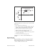
USER GUIDE USB-6501 OEM This user guide describes how to use the National Instruments USB-6501 OEM data acquisition (DAQ) device. The NI USB-6501 OEM is a full-speed USB 2.0 device that provides 24 DIO channels and a 32-bit counter. Dimensional Drawings Figure 1 shows a top view of the USB-6501 OEM. Figure 2 shows the front and rear dimensions. 0.45 in. (11.5 mm) 0.18 in. (4.5 mm) –0.03 in. (–0.8 mm) –0.18 in. (–4.6 mm) 2.26 in. (57.4 mm) 1.78 in. (45.2 mm) 1.61 in. (40.8 mm) 1.45 in. (36.7 mm) 1.37 in.
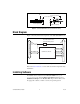
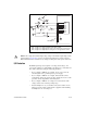
Pin 1 0.45 in. (11.5 mm) 0.25 in. (6.4 mm) 0.34 in. (8.6 mm) 0.06 in. (1.6 mm) Figure 2. USB-6501 OEM Dimensions (Front and Rear Views) Block Diagram Figure 3 shows key functional components of the USB-6501 OEM device. +5 V Vbus P2.<0..7> USB Microcontroller USB P1.<0..7> P0.<0..7> Digital I/O Terminal Block Full-Speed USB Interface Short Circuit Protection Current Limiting Circuit Figure 3.
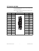
I/O Connector and Cable Use any 34-pin female IDC (ribbon) cable to connect to the IDC connector on the USB-6501 OEM device. Table 1 lists the pin assignments and signal names for the IDC connector. Table 1. Pin Assignments Signal Pin Connector Pin Signal P1.0 1 2 GND P1.1 3 4 P2.0 P1.2 5 6 GND P1.3 7 8 P2.1 P1.4 9 10 GND P1.5 11 12 P2.2 P1.6 13 14 GND P1.7 15 16 P2.3 P0.0 17 18 GND P0.1 19 20 P2.4 P0.2 21 22 GND P0.3 23 24 P2.5 P0.4 25 26 GND P0.
Signal Descriptions Table 2 describes the signals available on the I/O connectors. Table 2. Signal Descriptions Signal Name Direction Description P0.<0..7> P1.<0..7> P2.<0..6> Input or Output Digital I/O Signals—You can individually configure each signal as an input or output. P2.7 (CTR 0 SRC) Input or Output This pin is configurable as either a digital line or an event counter. Digital I/O Signal—As a digital line, this signal can be used as an input or output.
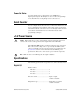
USB-6501 OEM DIO Box Short Circuit Protection Current Limiting Circuit +5 V Re VBus Rp 4.7K Onboard Resistor External Pull-up Resistor Port Pad P0.0 Rl Load GND A Figure 4. Example of Connecting External User-Provided Resistor Complete the following steps to determine the value of the user-provided pull-up resistor: 1. Place an ammeter in series with the load. 2. Place a variable resistor between the digital output line and the +5 V. 3.
+5 V 1 LED P0.0 P0.1 P0.2 P0.3 P0.4 P0.5 P0.6 P0.7 LED 2 3 +5 V TTL Signal 4 Switch GND I/O Connector 1 2 3 4 P0.0 configured as an open-drain digital output driving a LED P0.2 configured as a push-pull digital output driving a LED P0.4 configured as a digital input receiving a TTL signal from a gated inverter P0.7 configured as a digital input receiving a 0 V or 5 V signal from a switch Figure 5.
Power-On States At system startup and reset, the hardware sets all DIO lines to high-impedance inputs. The DAQ device does not drive the signal high or low. Each line has a weak pull-up resistor connected to it. Event Counter You can configure P2.7 as the source for a 32-bit counter. In this mode, the device counts high to low transitions on P2.7. The counter can be armed and disarmed and the count can be read or reset through software.
Pull-up resistor........................................4.7 kΩ VBus (nominally 5 V) Absolute voltage range ...........................–0.5 to 5.8 V with respect to GND Power-on state ........................................Input (high impedance) Digital logic levels Level Input Input low voltage Input high voltage Input leakage current Output Output low voltage (I = 8.5 mA) Output high voltage Push-pull, I = –8.5 mA Open-drain, I = –0.6 mA, nominal Open-drain, I = –8.
Power Requirements USB 4.10 to 5.25 VDC ............................ 80 mA typical, 500 mA max USB Suspend .................................. 300 µA standby mode, 500 µA max Physical Characteristics Dimensions ............................................ 5.74 cm × 6.73 cm × 1.15 cm (2.26 in. × 2.65 in. × 0.45 in.) I/O connectors ........................................ USB series B receptacle; 34-pin IDC ribbon cable header Weight .................................................... 21 g (.
specially protected secondary circuits. Such voltage measurements include signal levels, special equipment, limited-energy parts of equipment, circuits powered by regulated low-voltage sources, and electronics. Do not use this module for connection to signals or for measurements within Measurement Categories II, III, or IV. Caution Hazardous Locations The USB-6501 is not certified for use in hazardous locations. Environmental The USB-6501 device is intended for indoor use only.
Refer to the Declaration of Conformity (DoC) for this product for any additional regulatory compliance information. To obtain the DoC for this product, visit ni.com/certification, search by model number or product line, and click the appropriate link in the Certification column. Note Safety Guidelines Caution Operate the hardware only as described in these operating instructions.
Avoid contact between your body and the connector block signal when hot swapping modules. Remove power from signal lines before connecting them to or disconnecting them from the device. Operate the device at or below the Measurement Category I1. Measurement circuits are subjected to working voltages2 and transient stresses (overvoltage) from the circuit to which they are connected during measurement or test.
Where to Go for Support The National Instruments Web site is your complete resource for technical support. At ni.com/support you have access to everything from troubleshooting and application development self-help resources to email and phone assistance from NI Application Engineers. National Instruments corporate headquarters is located at 11500 North Mopac Expressway, Austin, Texas, 78759-3504. National Instruments also has offices located around the world to help address your support needs.