USER GUIDE AND SPECIFICATIONS NI USB-6509 This document contains information about using the National Instruments USB-6509 data acquisition (DAQ) device with NI-DAQmx 8.7 and later. The NI USB-6509 is a bus-powered 96-channel, digital input/output (I/O) device. The NI USB-6509 features 96 TTL/CMOS-compatible digital I/O lines, a watchdog timer, digital input filtering and change detection, and output programmable power-up states.
DIO Signal Connection ....................................................................16 Protecting Inductive Loads...............................................................17 Sinking and Sourcing Examples.......................................................17 Driving a Relay <24 mA ...........................................................17 Driving a Relay >24 mA ...........................................................18 Driving SSRs..........................................................
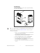
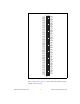
Installing the Hardware The NI-DAQmx for USB Devices Getting Started Guide contains non-software-specific information about how to install USB devices. USB Cable Strain Relief The two strain relief options for your USB cable are as follows: • Cable Strain Relief Groove Method—Press the USB cable into one of the two grooves on the underside of the NI USB-6509. Choose the USB cable groove that matches your USB cable size, as shown in Figure 1.
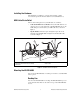
For secure desktop use, you can adhere the supplied rubber non-skid feet to the underside of the device, as shown in Figure 2. Do not apply the rubber feet if you are panel mounting the NI USB-6509 or stacking multiple NI USB-6509 devices. Note Figure 2. Applying Rubber Feet to the NI USB-6509 DIN Rail Mounting The DIN rail mounting kit (part number 779689-01, not included in your NI USB-6509 kit) is an accessory you can use to mount the NI USB-6509 to a standard DIN rail.
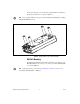
Panel Mounting To mount the NI USB-6509 to a board or panel, complete the following steps while referring to Figure 3. Figure 3. Mounting the NI USB-6509 on a Panel Notes Do not apply the rubber feet to the NI USB-6509 when panel mounting the device. Apply strain relief, as described in the USB Cable Strain Relief section, before panel mounting the NI USB-6509. 1. Go to ni.com/info and enter the info code rd3233 to download and print the panel mounting template PDF. 2.
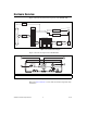
Hardware Overview Figure 4 shows the key functional components of the NI USB-6509.
Programming Devices in Software National Instruments measurement devices for USB are packaged with NI-DAQ driver software, an extensive library of functions and VIs you can call from your application software, such as LabVIEW or LabWindows™/CVI™, to program all the features of your NI measurement devices. Driver software has an application programming interface (API), which is a library of VIs, functions, classes, attributes, and properties for creating applications for your device. NI-DAQ 8.
Related Documentation The following documents contain information that you may find helpful as you use this user guide: • NI-DAQmx for USB Getting Started Guide—This guide describes how to install the NI-DAQmx software, the DAQ device, and how to confirm that the device is operating properly. • NI-DAQmx Help—This help file contains information about using NI-DAQmx to program National Instruments devices. NI-DAQmx is the software you use to communicate with and control NI DAQ devices.
P2.7 1 51 P8.7 P5.7 2 52 P11.7 P2.6 3 53 P8.6 P5.6 4 54 P11.6 P2.5 5 55 P8.5 P5.5 6 56 P11.5 P2.4 7 57 P8.4 P5.4 8 58 P11.4 P2.3 9 59 P8.3 P5.3 10 60 P11.3 P2.2 11 61 P8.2 P5.2 12 62 P11.2 P2.1 13 63 P8.1 P5.1 14 64 P11.1 P2.0 15 65 P8.0 P5.0 16 66 P11.0 P1.7 17 67 P7.7 P4.7 18 68 P10.7 P1.6 19 69 P7.6 P4.6 20 70 P10.6 P1.5 21 71 P7.5 P4.5 22 72 P10.5 P1.4 23 73 P7.4 P4.4 24 74 P10.4 P1.3 25 75 P7.3 P4.3 26 76 P10.3 P1.
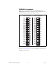
R1005050 Pin Assignments Figure 6 shows the pin assignments for the NI USB-6509 using the R1005050 cable. The naming convention for each pin is PX.Y, where X is the port (P) number, and Y is the line number or name. Positions 1 through 50 P2.7 P2.6 P2.5 P2.4 P2.3 P2.2 P2.1 P2.0 P1.7 P1.6 P1.5 P1.4 P1.3 P1.2 P1.1 P1.0 P0.7 P0.6 P0.5 P0.4 P0.3 P0.2 P0.1 P0.0 +5 V Positions 51 through 100 1 3 5 7 9 11 13 15 17 19 21 2 4 6 8 10 12 14 16 18 20 22 P5.7 P8.7 P5.6 P8.6 P5.5 P8.5 P5.4 P8.4 P5.3 P8.
Signal Descriptions Table 1 lists the signals and descriptions for all signals available on the NI USB-6509 device. Table 1. NI USB-6509 Signal Descriptions Pin Signal Name Description MSB LSB 1, 3, 5, 7, 9, 11, 13, 15 P2.<7..0> Bi-directional data lines for port 2 P2.7 P2.0 2, 4, 6, 8, 10, 12, 14, 16 P5.<7..0> Bi-directional data lines for port 5 P5.7 P5.0 17, 19, 21, 23, 25, 27, 29, 31 P1.<7..0> Bi-directional data lines for port 1 P1.7 P1.0 18, 20, 22, 24, 26, 28, 30, 32 P4.<7..
Digital I/O Static DIO on NI USB-6509 Devices You can use each of the NI USB-6509 DIO lines as a static digital input (DI) or digital output (DO) line. You can use static DIO lines to monitor or control digital signals. Each DIO port can be configured as a DI or DO port. All samples of static DI lines and updates of DO lines are software-timed. Digital I/O Circuitry The NI USB-6509 provides 96 lines of bidirectional DIO signals, P<0..11>.<0..7>.
conditioning solutions for digital applications requiring high current drive. • If you configure a DIO line as an input, do not drive the line with voltages outside of its normal operating range. • Treat the DAQ device as you would treat any static sensitive device. Always properly ground yourself and the equipment when handling the DAQ device or connecting to it. I/O State at Power-On/Power-Off/Suspend After the device is powered on, the default state of all I/O lines is input.
NI USB-6509 +5 V Transceiver 100 kΩ Digital I/O Line RL GND Figure 9. DIO Channel Configured for High DIO State with External Load Example: At power up, the device is configured for input and, by default, all DIO lines are high. To pull one channel low, complete the following steps: 1. Install a load (RL). Remember that the smaller the resistance, the greater the current consumption and the lower the voltage (V). 2.
Also, make sure the pull-up resistor value is not so large that leakage current from the DIO line brings the voltage at the resistor below a TTL-high level of 2 V. NI USB-6509 +5 V Transceiver RL Digital I/O Line 100 kΩ GND Figure 10. DIO Channel Configured for Low DIO State with External Load Example: The switch is set in the low DIO state, which means all DIO lines are pulled low. If you want to pull one channel high, complete the following steps: 1. Install a load (RL).
The NI USB-6509 has a current-sense circuit on VBUS (USB power rail). If the output channels source more than the specified current, the current is limited. The two following occurrences indicate an overcurrent condition: • The inputs/outputs are disabled • The LED on the back panel is blinking If you want to increase the current drive capacity on the NI USB-6509, you can use an optional external +12 VDC power supply. For more information, refer to the Optional +12 VDC Power Supply Installation section.
Protecting Inductive Loads When inductive loads are connected to outputs, a large counter-electromotive force may occur at switching time because of the energy stored in the inductive load. These flyback voltages can damage the outputs and/or the power supply. To limit these flyback voltages at the inductive load, install a flyback diode across the inductive load. For best results, mount the flyback diode within 18 inches of the load.
PX.Y GND NI USB-6509 Figure 14. NI USB-6509 Sourcing Connection Example, <24 mA Driving a Relay >24 mA Figures 15 and 16 are examples of connecting the NI USB-6509 to a relay that requires more than 24 mA of current. These examples use an additional transistor circuit. Vcc PX.Y GND NI USB-6509 Figure 15. NI USB-6509 Sinking Connection Example, >24 mA Vcc PX.Y GND NI USB-6509 Figure 16. NI USB-6509 Sourcing Connection Example, >24 mA NI 6509 User Guide and Specifications 18 ni.
Driving SSRs Figure 17 shows an example of connecting the NI USB-6509 to a solid-state relay (SSR). Load DC + _ or AC PX.Y SSR GND NI USB-6509 Figure 17. NI USB-6509 SSR Connection Example LED Indicator The LED indicator, located on the device back panel, indicates device status. Table 2 shows the behavior of the LED. Table 2.
+5 V Power Available at I/O Connector Pins 49 and 99 supply +5 V power to the I/O connector. The power drawn from these two pins shares the power consumption with the transceivers. The I/O connector power has a fuse for overcurrent protection. This fuse is not customer replaceable. If the fuse is blown, return the device to NI for repair. The power pins, +5V and GND, connect to the computer power supply and are not isolated.
Internally, the filter uses two clocks: the sample clock and the filter clock. The sample clock has a frequency of 48 MHz that corresponds to a period of 20.83 ns. The filter clock is generated by a counter and has a period equal to one half of the specified timing interval. The input signal is sampled on each rising edge of the sample clock. However, a change in the input signal is recognized only if it maintains its new state for at least two consecutive rising edges of the filter clock.
Programmable Power-Up States At power-up, the output drives on the NI USB-6509 are disabled. All lines are user-configurable for high-impedance input, high output, or low output. User-configurable power-up states are useful for ensuring that the NI USB-6509 powers up in a known state. To use MAX (recommended) to program the power-up states, select the device and click the Properties button.
Change Detection Example Table 4 shows a change detection example for six bits of one port. Table 4. Change Detection Example Bit 7 6 5 4 Changes to detect 3 2 — — 1 0 Enable rising-edge detection yes yes yes yes no no yes no Enable falling-edge detection yes yes yes yes no no no yes This example assumes the following line connections: • Bits 7, 6, 5, and 4 are connected to data lines from a four-bit TTL output device.
The expiration signal that indicates an expired watchdog continues to assert until the watchdog is disarmed. After the watchdog timer expires, the NI USB-6509 ignores any writes until the watchdog timer is disarmed. When the watchdog timer is enabled and the computer enters a fault condition, ports that are set to tri-state remain tri-stated and do not go to user-defined safe states.
Power-on state........................................ Configured as inputs, pull-up/pull-down (selectable on the back panel switch) Pull-up/pull-down resistor...................... 100 kΩ ±5% Data transfers ......................................... Programmed I/O Digital Input Characteristics Level Min Max Input voltage 0V 5.0 V Input low voltage — 0.8 V Input high voltage 2.0 V — Input low current (Vin = 0 V) — –91.0 μA Input high current (Vin= 5 V) — 91.
The total current sinking/sourcing from one port cannot exceed 100 mA. Total current sourced by all DO lines simultaneously should not exceed 215 mA for bus-powered configuration. If more sourcing current is required, use an optional external power supply +5V power available at I/O connector (pins 49 and 99) ...............+4.1 to +5.2 V; 215 mA, maximum (Bus-powered); 0.5 A, maximum (with external power supply) The I/O connector power has a fuse for overcurrent protection.
Safety This product is designed to meet the requirements of the following standards of safety for electrical equipment for measurement, control, and laboratory use: • IEC 61010-1, EN 61010-1 • UL 61010-1, CSA 61010-1 Note For UL and other safety certifications, refer to the product label or visit ni.com/ certification, search by model number or product line, and click the appropriate link in the Certification column. Hazardous Locations The NI USB-6509 is not certified for use in hazardous locations.
CE Compliance This product meets the essential requirements of applicable European Directives, as amended for CE marking, as follows: • 2006/95/EC; Low-Voltage Directive (safety) • 2004/108/EC; Electromagnetic Compatibility Directive (EMC) Refer to the Declaration of Conformity (DoC) for this product for any additional regulatory compliance information. To obtain the DoC for this product, visit ni.
Safety Guidelines Caution Operate the hardware only as described in these operating instructions. The following section contains important safety information that you must follow when installing and using the NI USB-6509. Do not operate the NI USB-6509 in a manner not specified in this document. Misuse of the device can result in a hazard. You can compromise the safety protection built into the device if the device is damaged in any way. If the device is damaged, contact National Instruments for repair.
Operate the device at or below the Measurement Category I1. Measurement circuits are subjected to working voltages2 and transient stresses (overvoltage) from the circuit to which they are connected during measurement or test. Measurement categories establish standard impulse withstand voltage levels that commonly occur in electrical distribution systems.
Where to Go for Support The National Instruments Web site is your complete resource for technical support. At ni.com/support you have access to everything from troubleshooting and application development self-help resources to email and phone assistance from NI Application Engineers. A Declaration of Conformity (DoC) is our claim of compliance with the Council of the European Communities using the manufacturer’s declaration of conformity.