Computer-Based Instruments NI 5911 User Manual Digital Oscilloscope for PCI NI 5911 User Manual September 2000 Edition Part Number 322150B-01
Support Worldwide Technical Support and Product Information ni.
Important Information Warranty The NI 5911 is warranted against defects in materials and workmanship for a period of one year from the date of shipment, as evidenced by receipts or other documentation. National Instruments will, at its option, repair or replace equipment that proves to be defective during the warranty period. This warranty includes parts and labor.
Conventions The following conventions are used in this manual: » The » symbol leads you through nested menu items and dialog box options to a final action. The sequence File»Page Setup»Options directs you to pull down the File menu, select the Page Setup item, and select Options from the last dialog box. This icon denotes a note, which alerts you to important information. bold Bold text denotes items that you must select or click on in the software, such as menu items and dialog box options.
Contents Chapter 1 Taking Measurements with the NI 5911 Installing the NI 5911 ....................................................................................................1-1 Connecting Signals ........................................................................................................1-1 Acquiring Data with Your NI 5911 ...............................................................................1-3 Programmatically Controlling Your NI 5911.............................................
Contents RTSI Bus Trigger and Clock Lines ............................................................................... 2-14 PFI Lines ......................................................................................................... 2-14 PFI Lines as Inputs ........................................................................... 2-14 PFI Lines as Outputs......................................................................... 2-15 Synchronization ...............................................
Taking Measurements with the NI 5911 1 Thank you for buying a National Instruments 5911 digital oscilloscope with flexible resolution. This chapter provides information on installing, connecting signals to, and acquiring data from your NI 5911. Installing the NI 5911 There are two main steps involved in installation: 1. Install the NI-SCOPE driver software. You use this driver to write programs to control your NI 5911 in different application development environments (ADEs).
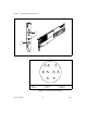
Chapter 1 Taking Measurements with the NI 5911 CH0 PFI1 PFI2 (DIN) Figure 1-1. NI 5911 Connectors 9 6 1 2 3 +5 Volts (Fused) GND Reserved 4 5 6 8 7 5 4 2 1 Reserved Reserved PFI 2 3 7 8 9 Reserved Reserved Reserved Figure 1-2. 9-Pin Mini Circular DIN Connector NI 5911 User Manual 1-2 ni.
Chapter 1 Taking Measurements with the NI 5911 The +5 V signal is fused at 1.1 A. However, National Instruments recommends limiting the current from this pin to 30 mA. The fuse is self-resetting. Note Acquiring Data with Your NI 5911 You can acquire data either programmatically—by writing an application for your NI 5911—or interactively with the VirtualBench-Scope soft front panel.
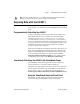
Chapter 1 Taking Measurements with the NI 5911 Acquiring Data When you launch VirtualBench-Scope, it operates in continuous run mode. To start acquiring signals with VirtualBench-Scope, complete the following steps: 1. Connect a signal to Channel 0 of your NI 5911. 2. Configure VirtualBench-Scope. a. From the Edit menu on the front panel, select General Settings. b. Select NI 5911 from the instrument list as shown in Figure 1-3.
Chapter 1 Taking Measurements with the NI 5911 When you launch VirtualBench-Scope, it automatically uses the settings of your previous VirtualBench-Scope session. Note 3. Enable the Ch 0 button in the channel selector area. Disable all other channels. Disabled channels have a gray frame around them. 4. Click Auto Setup on the main control bar. 5. Click Run to start the acquisition.
Chapter 1 Taking Measurements with the NI 5911 The VirtualBench-Scope soft front panel has the following features: • Channels selector—picks a channel or math functions that display waveforms. • Channel settings group: Channel settings selector selects the channel whose settings will be modified. – Coupling toggles between DC and AC coupling. – Volts/div adjusts the vertical resolution of the channel you select. – V. Position controls the displayed voltage offset.
2 Hardware Overview This chapter includes an overview of the NI 5911, explains the operation of each functional unit making up your NI 5911, and describes the signal connections. Figure 2-1 shows a block diagram of the NI 5911. Analog Input Connector AC/DC Coupling Protect/ Calibration Mux PGA A/D Converter 100 MHz, 8-bit Noise Shaper Calibration Generator Timing IO/ Memory Control Digital IO Connector Digital Signal Processor Capture Memory Reference Clock Data Figure 2-1.
Chapter 2 Hardware Overview Differential Input When measuring high dynamic range signals, ground noise is often a problem. The PGIA of the NI 5911 allows you to make noise-free signal measurements. The NI 5911 PGIA is a differential amplifier. The PGIA differential amplifier efficiently rejects any noise which may be present on the ground signal. Internal to the PGIA, the signal presented at the negative input is subtracted from the signal presented at the positive input.
Chapter 2 Hardware Overview Input Ranges To optimize the ADC resolution, you can select different gains for the PGIA. In this way, you can scale your input signal to match the full input range of the converter. The NI 5911 PGIA offers seven different input ranges, from ±0.1 V to ±10 V, as shown in Table 2-1. Table 2-1. Input Ranges for the NI 5911 Range Input Protection Threshold ±10 V ±10 V ±5 V ±5 V ±2 V ±5 V ±1 V ±5 V ±0.5 V ±5 V ±0.2 V ±5 V ±0.
Chapter 2 Hardware Overview Input Bias The inputs of the PGIA typically draw an input bias current of 1 nA at 25 °C. Attaching a device with a very high source impedance can cause an offset voltage to be added to the signal you measure, according to the formula Rs × 1 nA, where Rs is the external source impedance. For example, if the device you have attached to the NI 5911 has an output impedance of 10 kΩ, typically the offset voltage is 10 µV (10 kΩ ×1 nA).
Chapter 2 Hardware Overview Oscilloscope Mode The ADC converts at a constant rate of 100 MS/s, but you can choose to store only a fraction of these samples into memory at a lower rate. This allows you to store waveforms using fewer data points and decreases the burden of storing, analyzing, and displaying the waveforms. If you need faster sampling rates, you can use Random Interleaved Sampling (RIS) to effectively increase the sampling rate to 1 GS/s for repetitive waveforms.
Chapter 2 Hardware Overview Table 2-2. Available Sampling Rates and Corresponding Bandwidth in Flexible Resolution Mode (Continued) Sampling Rate Resolution Bandwidth 20 kS/s 20 bits 8 kHz 10 kS/s 21 bits 4 kHz Like any other type of converter that uses noise shaping to enhance resolution, the frequency response of the converter is only flat to its maximum useful bandwidth. The NI 5911 has a bandwidth of 4 MHz.
Chapter 2 Hardware Overview Internally Calibrating the NI 5911 Internally calibrate your NI 5911 with a software function or a LabVIEW VI. Read more about the function, niScope_CalSelfCalibrate, in your NI-SCOPE Function Reference Help file. LabVIEW users, see the context sensitive help (Help»Show Context Help) for niscope Cal Self Calibrate. vi.
Chapter 2 Hardware Overview of range and should be recalibrated by performing an internal calibration. During acquisition in flexible resolution mode, an error will be generated if the input to the ADC goes out of range for the converter. The fact that this condition has occurred may not be obvious by inspecting the acquired data due to the digital filtering that takes place on the acquired data.
Analog Input High Level Gain Low Level Chapter 2 Hardware Overview Analog Trigger Circuit ATC_OUT + COMP COMP – a. Analog Trigger Circuit Software ATC_OUT RTSI <0..6> PFI1, PFI2 Trigger 7 2 Arm b. Trigger and Arm Sources Figure 2-3. Trigger Sources Analog Trigger Circuit The analog trigger on the NI 5911 operates by comparing the current analog input to an onboard threshold voltage. This threshold voltage, the trigger value, can be set within the current input range in 170 steps.
Chapter 2 Hardware Overview Trigger Value Falling Edge Trigger Rising Edge Trigger Figure 2-4. Below-Level Analog Triggering Mode In below-level analog triggering mode, the trigger is generated when the signal value is less than the trigger value. Trigger Value Falling Edge Trigger Rising Edge Trigger Figure 2-5. Above-Level Analog Triggering Mode In above-level analog triggering mode, the trigger is generated when the signal value is greater than trigger value. NI 5911 User Manual 2-10 ni.
Chapter 2 Hardware Overview Trigger Value Hysteresis Value Trigger Falling Edge Trigger Rising Edge Trigger Figure 2-6. High-Hysteresis Analog Triggering Mode In high-hysteresis analog triggering mode, the trigger is generated when a signal crosses above the hysteresis value and then crosses above the trigger value. The signal must cross back below the hysteresis value before another trigger is generated. Hysteresis Value Trigger Value Trigger Falling Edge Trigger Rising Edge Trigger Figure 2-7.
Chapter 2 Hardware Overview Trigger Hold-Off The trigger hold-off is a length of time that the NI 5911 waits after a trigger is accepted before it accepts another trigger. In other words, when a trigger is received during acquisition, the trigger counter is loaded with the desired hold-off time. Hardware then rejects all triggers until the counter has expired or the current acquisition completes, whichever is longer.
Chapter 2 Hardware Overview Memory The NI 5911 stores samples in onboard memory before transferring the samples to the host computer. The minimum size for a buffer in the onboard memory is approximately 4,000 8-bit oscilloscope mode samples or 1,000 32-bit decimation mode samples. Software allows you to specify buffers of less than these minimum sizes.
Chapter 2 Hardware Overview 1 Trigger 2 3 Acquisition In Progress Buffer 1 1 2 2 = Trigger Not Accepted (Pretrigger Points Not Acquired) = Trigger Not Accepted (5 µs Dead Time) 3= Trigger Not Accepted (Acquisition in Progress) = Trigger Accepted Figure 2-9. Multiple Buffer Acquisition RTSI Bus Trigger and Clock Lines The RTSI bus allows National Instruments boards to synchronize timing and triggering on multiple devices.
Chapter 2 Hardware Overview PFI Lines as Outputs You can select PFI1 or PFI2 to output several digital signals. Reference Clock is a 10 MHz clock that is synchronous to the 100 MHz sample clock on the NI 5911. You can use the reference clock to synchronize to another NI 5911 configured as a slave device or to other equipment that can accept a 10 MHz reference. Frequency Output is a 1 kHz digital pulse train signal with a 50% duty cycle.
A Specifications This appendix lists the specifications of the NI 5911. These specifications are typical at 25 °C unless otherwise specified. Acquisition System Bandwidth .............................................. 100 MHz maximum, at all input ranges Number of channels ............................... 1 for PCI, 2 for VXI Number of flexible resolution ADC....... 1 for PCI, 2 for VXI Max sample rate ..................................... 1 GS/s repetitive, 100 MS/s single shot Sample onboard memory ....
Appendix A Specifications Sampling Frequency Mode Sample Depth (4 MB) Sample Depth (16 MB) 20 kHz Flexible Resolution 1 MS 4 MS 10 kHz Flexible Resolution 1 MS 4 MS * 1
Appendix A Specifications Max measurable input voltage ............... ±10 V (DC + peak AC) Input protection ...................................... ±42 VDC (DC + peak AC) Input bias current ................................... ±1 nA, typical at 25 °C Common-Mode Characteristics Impedance to chassis ground ................. 10 kΩ Common-mode rejection ratio ...............
Appendix A Specifications Dynamic Range Noise (excluding input-referred noise) Sampling Frequency Bandwidth Noise Density Total Noise 100 MHz/n 100 MHz –120 dBfs/ Hz –43 dBfs 12.5 MHz 3.75 MHz –135 dBfs/ Hz –64 dBfs 5 MHz 2 MHz –150 dBfs/ Hz –83 dBfs 2.
Appendix A Specifications Sampling Frequency SFDR for input 0 dBfs SFDR for input –20 dBfs SFDR for input –60 dBfs (typical) 20 kHz 100 dB 110 dB 160 dB 10 kHz 100 dB 110 dB 160 dB Timebase System Number of timebases ............................. 2, RTSI clock configured as a 10 MHz clock output (Master), or RTSI clock configured as a 10 MHz reference clock input (Slave). Clock accuracy (as Master).................... 10 MHz ±50 ppm Clock input tolerance (as Slave) ............
Appendix A Specifications Triggering Systems Modes .....................................................Above threshold, below threshold, between thresholds, outside thresholds Source .....................................................CH0, RTSI<0..6>, PFI 1,2 Slope .......................................................Rising/falling Hysteresis................................................
Appendix A Specifications Acquisition Modes RIS ......................................................... 1 GS/s down to 200 MS/s effective sample rate, repetitive signals only. Data is interleaved in software. RIS accuracy .......................................... <0.5 ns Single-shot ............................................. 100 MS/s down to 10 kS/s sample rate for transient and repetitive signals Power Requirements +5 VDC ................................................. 4 A +12 VDC ..............
Appendix A Specifications Calibration Internal....................................................Internal calibration is done upon software command. The calibration involves gain, offset and linearity correction for all input ranges and input modes. Interval.............................................1 week, or any time temperature changes beyond ±5 °C. Hardware detects temperature variations beyond calibration limits, which can also be queried by software. External......................................
B Digitizer Basics This appendix explains basic information you need to understand about making measurements with digitizers, including important terminology. Understanding Digitizers To understand how digitizers work, you should be familiar with the Nyquist theorem and how it affects analog bandwidth and sample rate. You should also understand terms including vertical sensitivity, analog-to-digital converter (ADC) resolution, record length, and triggering options.
Appendix B Digitizer Basics Analog Bandwidth Analog bandwidth describes the frequency range (in Hertz) in which a signal can be digitized accurately. This limitation is determined by the inherent frequency response of the input path which causes loss of amplitude and phase information. Analog bandwidth is the frequency at which the measured amplitude is 3 dB below the actual amplitude of the signal.
Appendix B Digitizer Basics 1µ = Sample Rate 2 MS/s = Sample Rate 20 MS/s Figure B-3. 1 MHz Sine Wave Sample Vertical Sensitivity Vertical sensitivity describes the smallest input voltage change the digitizer can capture. This limitation is because one distinct digital voltage encompasses a range of analog voltages. Therefore, it is possible that a minute change in voltage at the input is not noticeable at the output of the ADC.
Appendix B Digitizer Basics Range 0-5 V 111 110 101 100 011 010 001 000 0 5 V Voltage Fluctuations in This Region Will Be Unnoticed Figure B-4. Transfer Function of a 3-Bit ADC ADC Resolution ADC resolution limits the accuracy of a measurement. The higher the resolution (number of bits), the more accurate the measurement. An 8-bit ADC divides the vertical range of the input amplifier into 256 discrete levels.
Appendix B Digitizer Basics thresholds, programmable hysteresis values, and trigger hold-off. The NI 5911 also has two digital triggers that give you more flexibility in triggering by allowing you to connect a TTL/CMOS digital signal to trigger the acquisition. Random Interleaved Sampling Random Interleaved Sampling (RIS) is a form of Equivalent Time Sampling (ETS) that allows acquisition of pretriggered data.
Appendix B Digitizer Basics Frame 1 Frame 2 Frame 3 Trigger Level Input Signal Sample Times t1 t2 t3 t1 t2 t3 Figure B-5. Waveform Reconstruction with RIS The time measurement is made with a time-to-digital converter (TDC). The resolution of the TDC is the number of physical bins to which the TDC can quantize the trigger arrival time.
Appendix B Digitizer Basics For example, consider the maximum interpolation factor to be 5. If the TDC could output values from 0 to 15, then each logical bin will contain three physical bins, as shown in Figure B-6. Logical Bin Sample Clock 3 Physical Bins = 1 Logical Bin Desired Interpolation Factor = 5 Max Interpolation Factor = 15 Physical Bin Figure B-6.
Appendix B Digitizer Basics +127 LSB 0 LSB +7 LSB –8 LSB –128 LSB a. Gain = 1, Input Range ±5 V, Number of LSBs = 15 +127 LSB +38.4 LSB 0 LSB –38.4 LSB –128 LSB b. Gain = 5, Input Range ±1 V, Number of LSBs = 77 +153 LSB +127 LSB Acquired Signal 0 LSB –128 LSB –154 LSB c. Gain = 20, Input Range ±250 mV, Number of LSBs = 307.2 Figure B-7. Dynamic Range of an 8-Bit ADC with Three Different Gain Settings NI 5911 User Manual B-8 ni.
Appendix B Digitizer Basics • Source impedance—Most digitizers and digital storage oscilloscopes (DSOs) have a 1 MΩ input resistance in the passband. If the source impedance is large, the signal will be attenuated at the amplifier input and the measurement will be inaccurate. If the source impedance is unknown but suspected to be high, change the attenuation ratio on your probe and acquire data.
Appendix B Digitizer Basics +V 5V 1 2 3 4 Trigger Level t Hold-off Hold-off 1 and 3 = Trigger Accepted 2 and 4 = Trigger Ignored Figure B-8. Difficult Pulse Train Signal Ideally, the trigger event should occur at condition one, but sometimes the instrument may trigger on condition two because the signal crosses the trigger level.
Technical Support Resources C Web Support National Instruments Web support is your first stop for help in solving installation, configuration, and application problems and questions. Online problem-solving and diagnostic resources include frequently asked questions, knowledge bases, product-specific troubleshooting wizards, manuals, drivers, software updates, and more. Web support is available through the Technical Support section of ni.com NI Developer Zone The NI Developer Zone at ni.
Appendix C Technical Support Resources Worldwide Support National Instruments has offices located around the world to help address your support needs. You can access our branch office Web sites from the Worldwide Offices section of ni.com. Branch office Web sites provide up-to-date contact information, support phone numbers, e-mail addresses, and current events.
Glossary Prefix Meanings Value p- pico- 10 –12 n- nano- 10 –9 µ- micro- 10 – 6 m- milli- 10 –3 k- kilo- 10 3 M- mega- 10 6 G- giga- 10 9 Symbols % percent + positive of, or plus – negative of, or minus / per ° degree ± plus or minus Ω ohm A A amperes A/D analog to digital AC alternating current © National Instruments Corporation G-1 NI 5911 User Manual
Glossary AC coupled the passing of a signal through a filter network that removes the DC component of the signal ADC analog-to-digital converter—an electronic device, often an integrated circuit, that converts an analog voltage to a digital number ADC resolution the resolution of the ADC, which is measured in bits. An ADC with16 bits has a higher resolution, and thus a higher degree of accuracy, than a 12-bit ADC.
Glossary clock hardware component that controls timing for reading from or writing to groups CMRR common-mode rejection ratio—a measure of an instrument’s ability to reject interference from a common-mode signal, usually expressed in decibels (dB) counter/timer a circuit that counts external pulses or clock pulses (timing) coupling the manner in which a signal is connected from one location to another D dB decibel—the unit for expressing a logarithmic measure of the ratio of two signal levels: dB=
Glossary F filtering a type of signal conditioning that allows you to filter unwanted signals from the signal you are trying to measure G gain the factor by which a signal is amplified, sometimes expressed in decibels H hardware the physical components of a computer system, such as the circuit boards, plug-in boards, chassis, enclosures, peripherals, cables, and so on harmonics multiples of the fundamental frequency of a signal Hz hertz—per second, as in cycles per second or samples per second I
Glossary interrupt level the relative priority at which a device can interrupt ISA industry standard architecture K k kilo—the standard metric prefix for 1,000, or 103, used with units of measure such as volts, hertz, and meters kS 1,000 samples L LabVIEW laboratory virtual instrument engineering workbench—a graphical programming ADE developed by National Instruments LSB least significant bit M m meters MB megabytes of memory memory buffer see buffer MS million samples MSB most signifi
Glossary N noise an undesirable electrical signal—Noise comes from external sources such as the AC power line, motors, generators, transformers, fluorescent lights, soldering irons, CRT displays, computers, electrical storms, welders, radio transmitters, and internal sources such as semiconductors, resistors, and capacitors. Noise corrupts signals you are trying to send or receive. Nyquist frequency a frequency that is one-half the sampling rate.
Glossary pretriggering the technique used on a device to keep a buffer filled with data, so that when the trigger conditions are met, the sample includes the data leading up to the trigger condition PXI PCI eXtensions for Instrumentation. PXI is an open specification that builds off the CompactPCI specification by adding instrumentation-specific features.
Glossary sense in four-wire resistance the sense measures the voltage across the resistor being excited by the excitation current settling time the amount of time required for a voltage to reach its final value within specified limits source impedance a parameter of signal sources that reflects current-driving ability of voltage sources (lower is better) and the voltage-driving ability of current sources (higher is better) system noise a measure of the amount of noise seen by an analog circuit or an
Glossary V V volts VAC volts alternating current VDC volts direct current Verror voltage error VI virtual instrument—(1) a combination of hardware and/or software elements, typically used with a PC, that has the functionality of a classic stand-alone instrument (2) a LabVIEW software module (VI), which consists of a front panel user interface and a block diagram program Vrms volts, root mean square value W waveform shape the shape the magnitude of a signal creates over time working voltage t
Index Numbers B +5 V signal limitation on current (note), 1-3 self-resetting fuse (note), 1-3 bias, input, 2-4 block diagram of NI 5911, 2-1 BNC connector, 1-1 to 1-2 A C AC coupling, 2-4 accuracy characteristics, A-2 to A-3 accurate measurements for digitizers. See digitizers.
Index G noise-free signal measurement (figure), 2-2 digitizers, B-1 to B-10 ADC resolution, B-4 analog bandwidth, B-2 making accurate measurements, B-7 to B-10 dynamic range of 8-bit ADC (figure), B-8 general signal shape, B-9 to B-10 input coupling, B-10 input frequency, B-9 peak-to-peak value, B-7 to B-8 source impedance, B-9 trigger hold-off, B-10 Nyquist theorem, B-1 record length, B-4 sample rate, B-2 to B-3 triggering options, B-4 to B-5 vertical sensitivity, B-3 to B-4 DIN connector, 1-1 to 1-2 dis
Index I specifications, A-1 to A-8 acquisition characteristics, A-2 to A-5 acquisition modes, A-7 acquisition system, A-1 to A-2 timebase system, A-5 triggering systems, A-6 VirtualBench-Scope soft front panel, 1-2 to 1-6 Acquire tab (figure), 1-4 acquiring data, 1-4 to 1-5 features, 1-5 to 1-6 front panel (figure), 1-5 NI Developer Zone, C-1 NI-SCOPE driver software examples, 1-3 installing, 1-1 programmatically controlling NI 5911, 1-3 noise-free measurements, 2-2 Nyquist theorem, B-1 impedance formula
Index calibration, A-8 EMC compliance, A-7 operating environment, A-7 physical, A-7 power requirements, A-7 storage environment, A-7 timebase system, A-5 triggering systems, A-6 storage environment specifications, A-7 synchronization, 2-15 system integration, by National Instruments, C-1 power requirement specifications, A-7 programmatically controlling NI 5911, 1-3 pulse train signal, difficult (figure), B-10 R Random Interleaved Sampling (RIS) interpolation factor (figure), B-7 purpose and use, 2-5 spe
Index V W vertical sensitivity digitizers, B-3 to B-4 specifications, A-2 VirtualBench-Scope soft front panel, 1-2 to 1-6 Acquire tab (figure), 1-4 acquiring data, 1-4 to 1-5 features, 1-5 to 1-6 front panel (figure), 1-5 Web support from National Instruments, C-1 Worldwide technical support, C-2 © National Instruments Corporation I-5 NI 5911 User Manual