
DAQ 6023E/6024E/6025E Multifunction I/O Devices User Manual
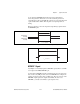
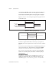
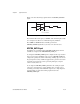
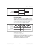
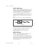
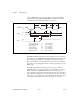
Table Of Contents
- 6023E/6024E/6025E User Manual
- Support
- Important Information
- Contents
- About This Manual
- Chapter 1 Introduction
- Chapter 2 Installation and Configuration
- Chapter 3 Hardware Overview
- Chapter 4 Signal Connections
- I/O Connector
- Analog Input Signal Overview
- Analog Input Signal Connections
- Analog Output Signal Connections
- Digital I/O Signal Connections
- Programmable Peripheral Interface (PPI)
- Power Connections
- Timing Connections
- Field Wiring Considerations
- Chapter 5 Calibration
- Appendix A Specifications
- Appendix B Custom Cabling and Optional Connectors
- Appendix C Common Questions
- Appendix D Technical Support Resources
- Glossary
- Index
- Figures
- Figure 1-1. The Relationship Between the Programming Environment, NI-DAQ, and Your Hardware
- Figure 3-1. PCI-6023E, PCI-6024E, PCI-6025E, and PXI-6025E Block Diagram
- Figure 3-2. DAQCard-6024E Block Diagram
- Figure 3-3. Dithering
- Figure 3-4. CONVERT* Signal Routing
- Figure 3-5. PCI RTSI Bus Signal Connection
- Figure 3-6. PXI RTSI Bus Signal Connection
- Figure 4-1. I/O Connector Pin Assignment for the 6023E/6024E
- Figure 4-2. I/O Connector Pin Assignment for the 6025E
- Figure 4-3. Programmable Gain Instrumentation Amplifier (PGIA)
- Figure 4-4. Summary of Analog Input Connections
- Figure 4-5. Differential Input Connections for Ground Referenced Signals
- Figure 4-6. Differential Input Connections for Nonreferenced Signals
- Figure 4-7. Single Ended Input Connections for Nonreferenced or Floating Signals
- Figure 4-8. Single Ended Input Connections for Ground Referenced Signals
- Figure 4-9. Analog Output Connections
- Figure 4-10. Digital I/O Connections
- Figure 4-11. Digital I/O Connections Block Diagram
- Figure 4-12. DIO Channel Configured for High DIO Power-up State with External Load
- Figure 4-13. Timing Specifications for Mode 1 Input Transfer
- Figure 4-14. Timing Specifications for Mode 1 Output Transfer
- Figure 4-15. Timing Specifications for Mode 2 Bidirectional Transfer
- Figure 4-16. Timing I/O Connections
- Figure 4-17. Typical Posttriggered Acquisition
- Figure 4-18. Typical Pretriggered Acquisition
- Figure 4-19. SCANCLK Signal Timing
- Figure 4-20. EXTSTROBE* Signal Timing
- Figure 4-21. TRIG1 Input Signal Timing
- Figure 4-22. TRIG1 Output Signal Timing
- Figure 4-23. TRIG2 Input Signal Timing
- Figure 4-24. TRIG2 Output Signal Timing
- Figure 4-25. STARTSCAN Input Signal Timing
- Figure 4-26. STARTSCAN Output Signal Timing
- Figure 4-27. CONVERT* Input Signal Timing
- Figure 4-28. CONVERT* Output Signal Timing
- Figure 4-29. SISOURCE Signal Timing
- Figure 4-30. WFTRIG Input Signal Timing
- Figure 4-31. WFTRIG Output Signal Timing
- Figure 4-32. UPDATE* Input Signal Timing
- Figure 4-33. UPDATE* Output Signal Timing
- Figure 4-34. UISOURCE Signal Timing
- Figure 4-35. GPCTR0_SOURCE Signal Timing
- Figure 4-36. GPCTR0_GATE Signal Timing in Edge Detection Mode
- Figure 4-37. GPCTR0_OUT Signal Timing
- Figure 4-38. GPCTR1_SOURCE Signal Timing
- Figure 4-39. GPCTR1_GATE Signal Timing in Edge Detection Mode
- Figure 4-40. GPCTR1_OUT Signal Timing
- Figure 4-41. GPCTR Timing Summary
- Figure B-1. 68 Pin E Series Connector Pin Assignments
- Figure B-2. 68 Pin Extended Digital Input Connector Pin Assignments
- Figure B-3. 50 Pin E Series Connector Pin Assignments
- Figure B-4. 50-Pin Extended Digital Input Connector Pin Assignments
- Tables
- Table 3-1. Available Input Configurations
- Table 3-2. Measurement Precision
- Table 3-3. Pins Used by PXI E Series Device
- Table 4-1. I/O Connector Details
- Table 4-2. I/O Connector Signal Descriptions
- Table 4-3. I/O Signal Summary
- Table 4-4. Port C Signal Assignments
- Table 4-5. Signal Names Used in Timing Diagrams

Chapter 4 Signal Connections
© National Instruments Corporation 4-49 6023E/6024E/6025E User Manual
If you use an internal timebase clock, the gate signal cannot be
synchronized with the clock. In this case, gates applied close to a source
edge take effect either on that source edge or on the next one. This
arrangement results in an uncertainty of one source clock period with
respect to unsynchronized gating sources.
The OUT output timing parameters are referenced to the signal at the
SOURCE input or to one of the internally generated clock signals on the
devices. Figure 4-41 shows the OUT signal referenced to the rising edge of
a source signal. Any OUT signal state changes occur within 80 ns after the
rising or falling edge of the source signal.
FREQ_OUT Signal
This signal is available only as an output on the FREQ_OUT pin. The
frequency generator of the device outputs the FREQ_OUT pin. The
frequency generator is a 4-bit counter that can divide its input clock by the
numbers 1 through 16. The input clock of the frequency generator is
software-selectable from the internal 10 MHz and 100 kHz timebases. The
output polarity is software-selectable. This output is set to high impedance
at startup.
Field Wiring Considerations
Environmental noise can seriously affect the accuracy of measurements
made with your device if you do not take proper care when running
signal wires between signal sources and the device. The following
recommendations apply mainly to analog input signal routing to the device,
although they also apply to signal routing in general.
Minimize noise pickup and maximize measurement accuracy by taking the
following precautions:
• Use DIFF analog input connections to reject common-mode noise.
• Use individually shielded, twisted-pair wires to connect analog input
signals to the device. With this type of wire, the signals attached to the
CH+ and CH– inputs are twisted together and then covered with a
shield. You then connect this shield only at one point to the signal
source ground. This kind of connection is required for signals traveling
through areas with large magnetic fields or high electromagnetic
interference.