
DAQ 6023E/6024E/6025E Multifunction I/O Devices User Manual
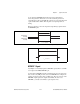
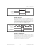
Table Of Contents
- 6023E/6024E/6025E User Manual
- Support
- Important Information
- Contents
- About This Manual
- Chapter 1 Introduction
- Chapter 2 Installation and Configuration
- Chapter 3 Hardware Overview
- Chapter 4 Signal Connections
- I/O Connector
- Analog Input Signal Overview
- Analog Input Signal Connections
- Analog Output Signal Connections
- Digital I/O Signal Connections
- Programmable Peripheral Interface (PPI)
- Power Connections
- Timing Connections
- Field Wiring Considerations
- Chapter 5 Calibration
- Appendix A Specifications
- Appendix B Custom Cabling and Optional Connectors
- Appendix C Common Questions
- Appendix D Technical Support Resources
- Glossary
- Index
- Figures
- Figure 1-1. The Relationship Between the Programming Environment, NI-DAQ, and Your Hardware
- Figure 3-1. PCI-6023E, PCI-6024E, PCI-6025E, and PXI-6025E Block Diagram
- Figure 3-2. DAQCard-6024E Block Diagram
- Figure 3-3. Dithering
- Figure 3-4. CONVERT* Signal Routing
- Figure 3-5. PCI RTSI Bus Signal Connection
- Figure 3-6. PXI RTSI Bus Signal Connection
- Figure 4-1. I/O Connector Pin Assignment for the 6023E/6024E
- Figure 4-2. I/O Connector Pin Assignment for the 6025E
- Figure 4-3. Programmable Gain Instrumentation Amplifier (PGIA)
- Figure 4-4. Summary of Analog Input Connections
- Figure 4-5. Differential Input Connections for Ground Referenced Signals
- Figure 4-6. Differential Input Connections for Nonreferenced Signals
- Figure 4-7. Single Ended Input Connections for Nonreferenced or Floating Signals
- Figure 4-8. Single Ended Input Connections for Ground Referenced Signals
- Figure 4-9. Analog Output Connections
- Figure 4-10. Digital I/O Connections
- Figure 4-11. Digital I/O Connections Block Diagram
- Figure 4-12. DIO Channel Configured for High DIO Power-up State with External Load
- Figure 4-13. Timing Specifications for Mode 1 Input Transfer
- Figure 4-14. Timing Specifications for Mode 1 Output Transfer
- Figure 4-15. Timing Specifications for Mode 2 Bidirectional Transfer
- Figure 4-16. Timing I/O Connections
- Figure 4-17. Typical Posttriggered Acquisition
- Figure 4-18. Typical Pretriggered Acquisition
- Figure 4-19. SCANCLK Signal Timing
- Figure 4-20. EXTSTROBE* Signal Timing
- Figure 4-21. TRIG1 Input Signal Timing
- Figure 4-22. TRIG1 Output Signal Timing
- Figure 4-23. TRIG2 Input Signal Timing
- Figure 4-24. TRIG2 Output Signal Timing
- Figure 4-25. STARTSCAN Input Signal Timing
- Figure 4-26. STARTSCAN Output Signal Timing
- Figure 4-27. CONVERT* Input Signal Timing
- Figure 4-28. CONVERT* Output Signal Timing
- Figure 4-29. SISOURCE Signal Timing
- Figure 4-30. WFTRIG Input Signal Timing
- Figure 4-31. WFTRIG Output Signal Timing
- Figure 4-32. UPDATE* Input Signal Timing
- Figure 4-33. UPDATE* Output Signal Timing
- Figure 4-34. UISOURCE Signal Timing
- Figure 4-35. GPCTR0_SOURCE Signal Timing
- Figure 4-36. GPCTR0_GATE Signal Timing in Edge Detection Mode
- Figure 4-37. GPCTR0_OUT Signal Timing
- Figure 4-38. GPCTR1_SOURCE Signal Timing
- Figure 4-39. GPCTR1_GATE Signal Timing in Edge Detection Mode
- Figure 4-40. GPCTR1_OUT Signal Timing
- Figure 4-41. GPCTR Timing Summary
- Figure B-1. 68 Pin E Series Connector Pin Assignments
- Figure B-2. 68 Pin Extended Digital Input Connector Pin Assignments
- Figure B-3. 50 Pin E Series Connector Pin Assignments
- Figure B-4. 50-Pin Extended Digital Input Connector Pin Assignments
- Tables
- Table 3-1. Available Input Configurations
- Table 3-2. Measurement Precision
- Table 3-3. Pins Used by PXI E Series Device
- Table 4-1. I/O Connector Details
- Table 4-2. I/O Connector Signal Descriptions
- Table 4-3. I/O Signal Summary
- Table 4-4. Port C Signal Assignments
- Table 4-5. Signal Names Used in Timing Diagrams
Chapter 4 Signal Connections
6023E/6024E/6025E User Manual 4-48 ni.com
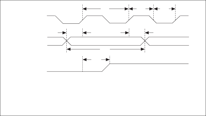
leave the DIO7 pin free for general use. Figure 4-41 shows the timing
requirements for the GATE and SOURCE input signals and the timing
specifications for the OUT output signals of your device.
Figure 4-41. GPCTR Timing Summary
The GATE and OUT signal transitions shown in Figure 4-41 are referenced
to the rising edge of the SOURCE signal. This timing diagram assumes that
the counters are programmed to count rising edges. The same timing
diagram, but with the source signal inverted and referenced to the falling
edge of the source signal, applies when the counter is programmed to count
falling edges.
The GATE input timing parameters are referenced to the signal at the
SOURCE input or to one of the internally generated signals on your device.
Figure 4-41 shows the GATE signal referenced to the rising edge of a
source signal. The gate must be valid (either high or low) for at least 10 ns
before the rising or falling edge of a source signal for the gate to take effect
at that source edge, as shown by t
gsu
and t
gh
in Figure 4-41. The gate signal
is not required to be held after the active edge of the source signal.
SOURCE
V
IH
V
IL
V
IH
V
IL
t
sc
t
sp
t
gsu
t
gh
t
gw
GATE
t
out
OUT
V
OH
V
OL
sc
t
t
t
t
t
t 50 ns minimum
sp
23 ns minimum
gsu
10 ns minimum
gh
0 ns minimum
gw
10 ns minimum
out
80 ns maximum
Source Clock Period
Source Pulse Width
Gate Setup Time
Gate Hold Time
Gate Pulse Width
Output Delay Time
t
sp