
DAQ 6023E/6024E/6025E Multifunction I/O Devices User Manual
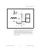
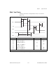
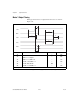
Table Of Contents
- 6023E/6024E/6025E User Manual
- Support
- Important Information
- Contents
- About This Manual
- Chapter 1 Introduction
- Chapter 2 Installation and Configuration
- Chapter 3 Hardware Overview
- Chapter 4 Signal Connections
- I/O Connector
- Analog Input Signal Overview
- Analog Input Signal Connections
- Analog Output Signal Connections
- Digital I/O Signal Connections
- Programmable Peripheral Interface (PPI)
- Power Connections
- Timing Connections
- Field Wiring Considerations
- Chapter 5 Calibration
- Appendix A Specifications
- Appendix B Custom Cabling and Optional Connectors
- Appendix C Common Questions
- Appendix D Technical Support Resources
- Glossary
- Index
- Figures
- Figure 1-1. The Relationship Between the Programming Environment, NI-DAQ, and Your Hardware
- Figure 3-1. PCI-6023E, PCI-6024E, PCI-6025E, and PXI-6025E Block Diagram
- Figure 3-2. DAQCard-6024E Block Diagram
- Figure 3-3. Dithering
- Figure 3-4. CONVERT* Signal Routing
- Figure 3-5. PCI RTSI Bus Signal Connection
- Figure 3-6. PXI RTSI Bus Signal Connection
- Figure 4-1. I/O Connector Pin Assignment for the 6023E/6024E
- Figure 4-2. I/O Connector Pin Assignment for the 6025E
- Figure 4-3. Programmable Gain Instrumentation Amplifier (PGIA)
- Figure 4-4. Summary of Analog Input Connections
- Figure 4-5. Differential Input Connections for Ground Referenced Signals
- Figure 4-6. Differential Input Connections for Nonreferenced Signals
- Figure 4-7. Single Ended Input Connections for Nonreferenced or Floating Signals
- Figure 4-8. Single Ended Input Connections for Ground Referenced Signals
- Figure 4-9. Analog Output Connections
- Figure 4-10. Digital I/O Connections
- Figure 4-11. Digital I/O Connections Block Diagram
- Figure 4-12. DIO Channel Configured for High DIO Power-up State with External Load
- Figure 4-13. Timing Specifications for Mode 1 Input Transfer
- Figure 4-14. Timing Specifications for Mode 1 Output Transfer
- Figure 4-15. Timing Specifications for Mode 2 Bidirectional Transfer
- Figure 4-16. Timing I/O Connections
- Figure 4-17. Typical Posttriggered Acquisition
- Figure 4-18. Typical Pretriggered Acquisition
- Figure 4-19. SCANCLK Signal Timing
- Figure 4-20. EXTSTROBE* Signal Timing
- Figure 4-21. TRIG1 Input Signal Timing
- Figure 4-22. TRIG1 Output Signal Timing
- Figure 4-23. TRIG2 Input Signal Timing
- Figure 4-24. TRIG2 Output Signal Timing
- Figure 4-25. STARTSCAN Input Signal Timing
- Figure 4-26. STARTSCAN Output Signal Timing
- Figure 4-27. CONVERT* Input Signal Timing
- Figure 4-28. CONVERT* Output Signal Timing
- Figure 4-29. SISOURCE Signal Timing
- Figure 4-30. WFTRIG Input Signal Timing
- Figure 4-31. WFTRIG Output Signal Timing
- Figure 4-32. UPDATE* Input Signal Timing
- Figure 4-33. UPDATE* Output Signal Timing
- Figure 4-34. UISOURCE Signal Timing
- Figure 4-35. GPCTR0_SOURCE Signal Timing
- Figure 4-36. GPCTR0_GATE Signal Timing in Edge Detection Mode
- Figure 4-37. GPCTR0_OUT Signal Timing
- Figure 4-38. GPCTR1_SOURCE Signal Timing
- Figure 4-39. GPCTR1_GATE Signal Timing in Edge Detection Mode
- Figure 4-40. GPCTR1_OUT Signal Timing
- Figure 4-41. GPCTR Timing Summary
- Figure B-1. 68 Pin E Series Connector Pin Assignments
- Figure B-2. 68 Pin Extended Digital Input Connector Pin Assignments
- Figure B-3. 50 Pin E Series Connector Pin Assignments
- Figure B-4. 50-Pin Extended Digital Input Connector Pin Assignments
- Tables
- Table 3-1. Available Input Configurations
- Table 3-2. Measurement Precision
- Table 3-3. Pins Used by PXI E Series Device
- Table 4-1. I/O Connector Details
- Table 4-2. I/O Connector Signal Descriptions
- Table 4-3. I/O Signal Summary
- Table 4-4. Port C Signal Assignments
- Table 4-5. Signal Names Used in Timing Diagrams
Chapter 4 Signal Connections
6023E/6024E/6025E User Manual 4-24 ni.com
Power-up State
♦ 6025E only
The 6025E contains bias resistors that control the state of the digital I/O
lines PA<0..7>,PB<0..7>,PC<0..7> at power up. Each digital I/O line is
configured as an input, pulled high by a 100 kΩ bias resistor.
You can change individual lines from pulled up to pulled down by adding
your own external resistors. This section describes the procedure.
Changing DIO Power-up State to Pulled Low
Each DIO line is pulled to V
cc
(approximately +5 VDC) with a 100 kΩ
resistor. To pull a specific line low, connect between that line and ground
a pull-down resistor (R
L
) whose value gives you a maximum of 0.4 VDC.
The DIO lines provide a maximum of 2.5 mA at 3.7 V in the high state.
Using the largest possible resistor ensures that you do not use more current
than necessary to perform the pull-down task.
However, make sure the value of the resistor is not so large that leakage
current from the DIO line along with the current from the 100 kΩ pull-up
resistor drives the voltage at the resistor above a TTL-low level of 0.4 VDC.
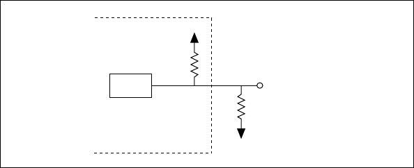
Figure 4-12 shows the DIO configuration for high DIO power-up state.
Figure 4-12. DIO Channel Configured for High DIO Power-up State with External Load
Example
A given DIO line is pulled high at power up. To pull it low on power up with
an external resistor, follow these steps:
1. Install a load (R
L
). Remember that the smaller the resistance, the
greater the current consumption and the lower the voltage.
Device
Digital I/O Line
82C55
100 k
GND
R
L
+5 V