
DAQ 6023E/6024E/6025E Multifunction I/O Devices User Manual
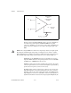
Table Of Contents
- 6023E/6024E/6025E User Manual
- Support
- Important Information
- Contents
- About This Manual
- Chapter 1 Introduction
- Chapter 2 Installation and Configuration
- Chapter 3 Hardware Overview
- Chapter 4 Signal Connections
- I/O Connector
- Analog Input Signal Overview
- Analog Input Signal Connections
- Analog Output Signal Connections
- Digital I/O Signal Connections
- Programmable Peripheral Interface (PPI)
- Power Connections
- Timing Connections
- Field Wiring Considerations
- Chapter 5 Calibration
- Appendix A Specifications
- Appendix B Custom Cabling and Optional Connectors
- Appendix C Common Questions
- Appendix D Technical Support Resources
- Glossary
- Index
- Figures
- Figure 1-1. The Relationship Between the Programming Environment, NI-DAQ, and Your Hardware
- Figure 3-1. PCI-6023E, PCI-6024E, PCI-6025E, and PXI-6025E Block Diagram
- Figure 3-2. DAQCard-6024E Block Diagram
- Figure 3-3. Dithering
- Figure 3-4. CONVERT* Signal Routing
- Figure 3-5. PCI RTSI Bus Signal Connection
- Figure 3-6. PXI RTSI Bus Signal Connection
- Figure 4-1. I/O Connector Pin Assignment for the 6023E/6024E
- Figure 4-2. I/O Connector Pin Assignment for the 6025E
- Figure 4-3. Programmable Gain Instrumentation Amplifier (PGIA)
- Figure 4-4. Summary of Analog Input Connections
- Figure 4-5. Differential Input Connections for Ground Referenced Signals
- Figure 4-6. Differential Input Connections for Nonreferenced Signals
- Figure 4-7. Single Ended Input Connections for Nonreferenced or Floating Signals
- Figure 4-8. Single Ended Input Connections for Ground Referenced Signals
- Figure 4-9. Analog Output Connections
- Figure 4-10. Digital I/O Connections
- Figure 4-11. Digital I/O Connections Block Diagram
- Figure 4-12. DIO Channel Configured for High DIO Power-up State with External Load
- Figure 4-13. Timing Specifications for Mode 1 Input Transfer
- Figure 4-14. Timing Specifications for Mode 1 Output Transfer
- Figure 4-15. Timing Specifications for Mode 2 Bidirectional Transfer
- Figure 4-16. Timing I/O Connections
- Figure 4-17. Typical Posttriggered Acquisition
- Figure 4-18. Typical Pretriggered Acquisition
- Figure 4-19. SCANCLK Signal Timing
- Figure 4-20. EXTSTROBE* Signal Timing
- Figure 4-21. TRIG1 Input Signal Timing
- Figure 4-22. TRIG1 Output Signal Timing
- Figure 4-23. TRIG2 Input Signal Timing
- Figure 4-24. TRIG2 Output Signal Timing
- Figure 4-25. STARTSCAN Input Signal Timing
- Figure 4-26. STARTSCAN Output Signal Timing
- Figure 4-27. CONVERT* Input Signal Timing
- Figure 4-28. CONVERT* Output Signal Timing
- Figure 4-29. SISOURCE Signal Timing
- Figure 4-30. WFTRIG Input Signal Timing
- Figure 4-31. WFTRIG Output Signal Timing
- Figure 4-32. UPDATE* Input Signal Timing
- Figure 4-33. UPDATE* Output Signal Timing
- Figure 4-34. UISOURCE Signal Timing
- Figure 4-35. GPCTR0_SOURCE Signal Timing
- Figure 4-36. GPCTR0_GATE Signal Timing in Edge Detection Mode
- Figure 4-37. GPCTR0_OUT Signal Timing
- Figure 4-38. GPCTR1_SOURCE Signal Timing
- Figure 4-39. GPCTR1_GATE Signal Timing in Edge Detection Mode
- Figure 4-40. GPCTR1_OUT Signal Timing
- Figure 4-41. GPCTR Timing Summary
- Figure B-1. 68 Pin E Series Connector Pin Assignments
- Figure B-2. 68 Pin Extended Digital Input Connector Pin Assignments
- Figure B-3. 50 Pin E Series Connector Pin Assignments
- Figure B-4. 50-Pin Extended Digital Input Connector Pin Assignments
- Tables
- Table 3-1. Available Input Configurations
- Table 3-2. Measurement Precision
- Table 3-3. Pins Used by PXI E Series Device
- Table 4-1. I/O Connector Details
- Table 4-2. I/O Connector Signal Descriptions
- Table 4-3. I/O Signal Summary
- Table 4-4. Port C Signal Assignments
- Table 4-5. Signal Names Used in Timing Diagrams
Chapter 4 Signal Connections
© National Instruments Corporation 4-9 6023E/6024E/6025E User Manual
Floating Signal Sources
A floating signal source is not connected in any way to the building ground
system, but has an isolated ground-reference point. Some examples of
floating signal sources are outputs of transformers, thermocouples,
battery-powered devices, optical isolators, and isolation amplifiers. An
instrument or device that has an isolated output is a floating signal source.
You must tie the ground reference of a floating signal to the analog input
ground of your device to establish a local or onboard reference for the
signal. Otherwise, the measured input signal varies as the source floats out
of the common-mode input range.
Ground-Referenced Signal Sources
A ground-referenced signal source is connected in some way to the
building system ground and is, therefore, already connected to a common
ground point with respect to the device, assuming that the computer is
plugged into the same power system. Non-isolated outputs of instruments
and devices that plug into the building power system fall into this category.
The difference in ground potential between two instruments connected to
the same building power system is typically between 1 and 100 mV, but can
be much higher if power distribution circuits are not properly connected.
If a grounded signal source is improperly measured, this difference can
appear as an error in the measurement. The connection instructions for
grounded signal sources are designed to eliminate this ground potential
difference from the measured signal.
Analog Input Modes
You can configure your device for one of three input
modes—nonreferenced single ended (NRSE), referenced single ended
(RSE), and differential (DIFF). With the different configurations, you can
use the PGIA in different ways. Figure 4-3 shows a diagram of the PGIA
of your device.