
DAQ 6023E/6024E/6025E Multifunction I/O Devices User Manual
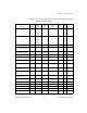
Table Of Contents
- 6023E/6024E/6025E User Manual
- Support
- Important Information
- Contents
- About This Manual
- Chapter 1 Introduction
- Chapter 2 Installation and Configuration
- Chapter 3 Hardware Overview
- Chapter 4 Signal Connections
- I/O Connector
- Analog Input Signal Overview
- Analog Input Signal Connections
- Analog Output Signal Connections
- Digital I/O Signal Connections
- Programmable Peripheral Interface (PPI)
- Power Connections
- Timing Connections
- Field Wiring Considerations
- Chapter 5 Calibration
- Appendix A Specifications
- Appendix B Custom Cabling and Optional Connectors
- Appendix C Common Questions
- Appendix D Technical Support Resources
- Glossary
- Index
- Figures
- Figure 1-1. The Relationship Between the Programming Environment, NI-DAQ, and Your Hardware
- Figure 3-1. PCI-6023E, PCI-6024E, PCI-6025E, and PXI-6025E Block Diagram
- Figure 3-2. DAQCard-6024E Block Diagram
- Figure 3-3. Dithering
- Figure 3-4. CONVERT* Signal Routing
- Figure 3-5. PCI RTSI Bus Signal Connection
- Figure 3-6. PXI RTSI Bus Signal Connection
- Figure 4-1. I/O Connector Pin Assignment for the 6023E/6024E
- Figure 4-2. I/O Connector Pin Assignment for the 6025E
- Figure 4-3. Programmable Gain Instrumentation Amplifier (PGIA)
- Figure 4-4. Summary of Analog Input Connections
- Figure 4-5. Differential Input Connections for Ground Referenced Signals
- Figure 4-6. Differential Input Connections for Nonreferenced Signals
- Figure 4-7. Single Ended Input Connections for Nonreferenced or Floating Signals
- Figure 4-8. Single Ended Input Connections for Ground Referenced Signals
- Figure 4-9. Analog Output Connections
- Figure 4-10. Digital I/O Connections
- Figure 4-11. Digital I/O Connections Block Diagram
- Figure 4-12. DIO Channel Configured for High DIO Power-up State with External Load
- Figure 4-13. Timing Specifications for Mode 1 Input Transfer
- Figure 4-14. Timing Specifications for Mode 1 Output Transfer
- Figure 4-15. Timing Specifications for Mode 2 Bidirectional Transfer
- Figure 4-16. Timing I/O Connections
- Figure 4-17. Typical Posttriggered Acquisition
- Figure 4-18. Typical Pretriggered Acquisition
- Figure 4-19. SCANCLK Signal Timing
- Figure 4-20. EXTSTROBE* Signal Timing
- Figure 4-21. TRIG1 Input Signal Timing
- Figure 4-22. TRIG1 Output Signal Timing
- Figure 4-23. TRIG2 Input Signal Timing
- Figure 4-24. TRIG2 Output Signal Timing
- Figure 4-25. STARTSCAN Input Signal Timing
- Figure 4-26. STARTSCAN Output Signal Timing
- Figure 4-27. CONVERT* Input Signal Timing
- Figure 4-28. CONVERT* Output Signal Timing
- Figure 4-29. SISOURCE Signal Timing
- Figure 4-30. WFTRIG Input Signal Timing
- Figure 4-31. WFTRIG Output Signal Timing
- Figure 4-32. UPDATE* Input Signal Timing
- Figure 4-33. UPDATE* Output Signal Timing
- Figure 4-34. UISOURCE Signal Timing
- Figure 4-35. GPCTR0_SOURCE Signal Timing
- Figure 4-36. GPCTR0_GATE Signal Timing in Edge Detection Mode
- Figure 4-37. GPCTR0_OUT Signal Timing
- Figure 4-38. GPCTR1_SOURCE Signal Timing
- Figure 4-39. GPCTR1_GATE Signal Timing in Edge Detection Mode
- Figure 4-40. GPCTR1_OUT Signal Timing
- Figure 4-41. GPCTR Timing Summary
- Figure B-1. 68 Pin E Series Connector Pin Assignments
- Figure B-2. 68 Pin Extended Digital Input Connector Pin Assignments
- Figure B-3. 50 Pin E Series Connector Pin Assignments
- Figure B-4. 50-Pin Extended Digital Input Connector Pin Assignments
- Tables
- Table 3-1. Available Input Configurations
- Table 3-2. Measurement Precision
- Table 3-3. Pins Used by PXI E Series Device
- Table 4-1. I/O Connector Details
- Table 4-2. I/O Connector Signal Descriptions
- Table 4-3. I/O Signal Summary
- Table 4-4. Port C Signal Assignments
- Table 4-5. Signal Names Used in Timing Diagrams
Chapter 4 Signal Connections
6023E/6024E/6025E User Manual 4-8 ni.com
Analog Input Signal Overview
The analog input signals for these devices are ACH<0..15>, ASENSE, and
AIGND. Connection of these analog input signals to your device depends
on the type of input signal source and the configuration of the analog input
channels you are using. This section provides an overview of the different
types of signal sources and analog input configuration modes. More
specific signal connection information is provided in the Analog Input
Signal Connections section.
Types of Signal Sources
When configuring the input channels and making signal connections,
you must first determine whether the signal sources are floating or
ground-referenced.
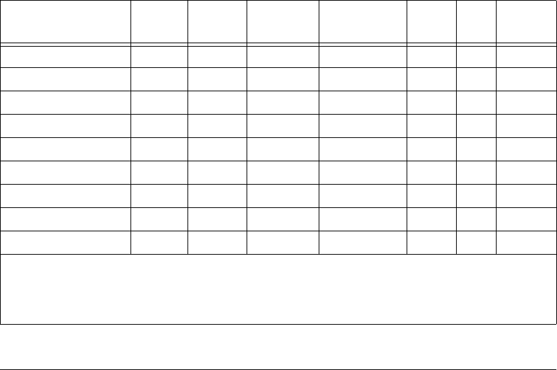
PFI4/GPCTR1_GATE DIO — V
cc
+0.5 3.5 at (V
cc
-0.4) 5at0.4 1.5 50 kΩ pu
GPCTR1_OUT DO — — 3.5 at (V
cc
-0.4) 5at0.4 1.5 50 kΩ pu
PFI5/UPDATE* DIO — V
cc
+0.5 3.5 at (V
cc
-0.4) 5at0.4 1.5 50 kΩ pu
PFI6/WFTRIG DIO — V
cc
+0.5 3.5 at (V
cc
-0.4) 5at0.4 1.5 50 kΩ pu
PFI7/STARTSCAN DIO — V
cc
+0.5 3.5 at (V
cc
-0.4) 5at0.4 1.5 50 kΩ pu
PFI8/GPCTR0_SOURCE DIO — V
cc
+0.5 3.5 at (V
cc
-0.4) 5at0.4 1.5 50 kΩ pu
PFI9/GPCTR0_GATE DIO — V
cc
+0.5 3.5 at (V
cc
-0.4) 5at0.4 1.5 50 kΩ pu
GPCTR0_OUT DO — — 3.5 at (V
cc
-0.4) 5at0.4 1.5 50 kΩ pu
FREQ_OUT DO — — 3.5 at (V
cc
-0.4) 5at0.4 1.5 50 kΩ pu
AI = Analog Input DIO = Digital Input/Output pu = pullup
AO = Analog Output DO = Digital Output
Note: The tolerance on the 50 kΩ pullup and pulldown resistors is very large. Actual value can range between 17 kΩ and
100 kΩ.
Table 4-3. I/O Signal Summary (Continued)
Signal Name
Signal
Type and
Direction
Impedance
Input/
Output
Protection
(Volts)
On/Off
Source
(mA at V)
Sink
(mA
at V)
Rise
Time
(ns)
Bias