
DAQ 6023E/6024E/6025E Multifunction I/O Devices User Manual
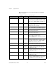
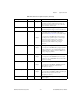
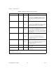
Table Of Contents
- 6023E/6024E/6025E User Manual
- Support
- Important Information
- Contents
- About This Manual
- Chapter 1 Introduction
- Chapter 2 Installation and Configuration
- Chapter 3 Hardware Overview
- Chapter 4 Signal Connections
- I/O Connector
- Analog Input Signal Overview
- Analog Input Signal Connections
- Analog Output Signal Connections
- Digital I/O Signal Connections
- Programmable Peripheral Interface (PPI)
- Power Connections
- Timing Connections
- Field Wiring Considerations
- Chapter 5 Calibration
- Appendix A Specifications
- Appendix B Custom Cabling and Optional Connectors
- Appendix C Common Questions
- Appendix D Technical Support Resources
- Glossary
- Index
- Figures
- Figure 1-1. The Relationship Between the Programming Environment, NI-DAQ, and Your Hardware
- Figure 3-1. PCI-6023E, PCI-6024E, PCI-6025E, and PXI-6025E Block Diagram
- Figure 3-2. DAQCard-6024E Block Diagram
- Figure 3-3. Dithering
- Figure 3-4. CONVERT* Signal Routing
- Figure 3-5. PCI RTSI Bus Signal Connection
- Figure 3-6. PXI RTSI Bus Signal Connection
- Figure 4-1. I/O Connector Pin Assignment for the 6023E/6024E
- Figure 4-2. I/O Connector Pin Assignment for the 6025E
- Figure 4-3. Programmable Gain Instrumentation Amplifier (PGIA)
- Figure 4-4. Summary of Analog Input Connections
- Figure 4-5. Differential Input Connections for Ground Referenced Signals
- Figure 4-6. Differential Input Connections for Nonreferenced Signals
- Figure 4-7. Single Ended Input Connections for Nonreferenced or Floating Signals
- Figure 4-8. Single Ended Input Connections for Ground Referenced Signals
- Figure 4-9. Analog Output Connections
- Figure 4-10. Digital I/O Connections
- Figure 4-11. Digital I/O Connections Block Diagram
- Figure 4-12. DIO Channel Configured for High DIO Power-up State with External Load
- Figure 4-13. Timing Specifications for Mode 1 Input Transfer
- Figure 4-14. Timing Specifications for Mode 1 Output Transfer
- Figure 4-15. Timing Specifications for Mode 2 Bidirectional Transfer
- Figure 4-16. Timing I/O Connections
- Figure 4-17. Typical Posttriggered Acquisition
- Figure 4-18. Typical Pretriggered Acquisition
- Figure 4-19. SCANCLK Signal Timing
- Figure 4-20. EXTSTROBE* Signal Timing
- Figure 4-21. TRIG1 Input Signal Timing
- Figure 4-22. TRIG1 Output Signal Timing
- Figure 4-23. TRIG2 Input Signal Timing
- Figure 4-24. TRIG2 Output Signal Timing
- Figure 4-25. STARTSCAN Input Signal Timing
- Figure 4-26. STARTSCAN Output Signal Timing
- Figure 4-27. CONVERT* Input Signal Timing
- Figure 4-28. CONVERT* Output Signal Timing
- Figure 4-29. SISOURCE Signal Timing
- Figure 4-30. WFTRIG Input Signal Timing
- Figure 4-31. WFTRIG Output Signal Timing
- Figure 4-32. UPDATE* Input Signal Timing
- Figure 4-33. UPDATE* Output Signal Timing
- Figure 4-34. UISOURCE Signal Timing
- Figure 4-35. GPCTR0_SOURCE Signal Timing
- Figure 4-36. GPCTR0_GATE Signal Timing in Edge Detection Mode
- Figure 4-37. GPCTR0_OUT Signal Timing
- Figure 4-38. GPCTR1_SOURCE Signal Timing
- Figure 4-39. GPCTR1_GATE Signal Timing in Edge Detection Mode
- Figure 4-40. GPCTR1_OUT Signal Timing
- Figure 4-41. GPCTR Timing Summary
- Figure B-1. 68 Pin E Series Connector Pin Assignments
- Figure B-2. 68 Pin Extended Digital Input Connector Pin Assignments
- Figure B-3. 50 Pin E Series Connector Pin Assignments
- Figure B-4. 50-Pin Extended Digital Input Connector Pin Assignments
- Tables
- Table 3-1. Available Input Configurations
- Table 3-2. Measurement Precision
- Table 3-3. Pins Used by PXI E Series Device
- Table 4-1. I/O Connector Details
- Table 4-2. I/O Connector Signal Descriptions
- Table 4-3. I/O Signal Summary
- Table 4-4. Port C Signal Assignments
- Table 4-5. Signal Names Used in Timing Diagrams

Chapter 4 Signal Connections
6023E/6024E/6025E User Manual 4-6 ni.com
PFI5/UPDATE* DGND Input
Output
PFI5/Update—as an input, this is one of the PFIs.
As an output, this is the UPDATE* (AO Update) signal. A
high-to-low edge on UPDATE* indicates that the analog
output primary group is being updated for the 6024E or
6025E.
PFI6/WFTRIG DGND Input
Output
PFI6/Waveform Trigger—as an input, this is one of the
PFIs.
As an output, this is the WFTRIG (AO Start Trigger) signal.
In timed analog output sequences, a low-to-high transition
indicates the initiation of the waveform generation.
PFI7/STARTSCAN DGND Input
Output
PFI7/Start of Scan—as an input, this is one of the PFIs.
As an output, this is the STARTSCAN (AI Scan Start)
signal. This pin pulses once at the start of each analog input
scan in the interval scan. A low-to-high transition indicates
the start of the scan.
PFI8/GPCTR0_SOURCE DGND Input
Output
PFI8/Counter 0 Source—as an input, this is one of the
PFIs.
As an output, this is the GPCTR0_SOURCE signal.
This signal reflects the actual source connected to the
general-purpose counter 0.
PFI9/GPCTR0_GATE DGND Input
Output
PFI9/Counter 0 Gate—as an input, this is one of the PFIs.
As an output, this is the GPCTR0_GATE signal. This signal
reflects the actual gate signal connected to the
general-purpose counter 0.
GPCTR0_OUT DGND Output Counter 0 Output—this output is from the general-purpose
counter 0 output.
FREQ_OUT DGND Output Frequency Output—this output is from the frequency
generator output.
*
Indicates that the signal is active low
1
Not available on the 6023E
2
Not available on the 6023E or 6024E
Table 4-2. I/O Connector Signal Descriptions (Continued)
Signal Name Reference Direction Description