
DAQ 6023E/6024E/6025E Multifunction I/O Devices User Manual
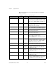
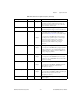
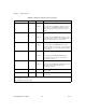
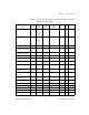
Table Of Contents
- 6023E/6024E/6025E User Manual
- Support
- Important Information
- Contents
- About This Manual
- Chapter 1 Introduction
- Chapter 2 Installation and Configuration
- Chapter 3 Hardware Overview
- Chapter 4 Signal Connections
- I/O Connector
- Analog Input Signal Overview
- Analog Input Signal Connections
- Analog Output Signal Connections
- Digital I/O Signal Connections
- Programmable Peripheral Interface (PPI)
- Power Connections
- Timing Connections
- Field Wiring Considerations
- Chapter 5 Calibration
- Appendix A Specifications
- Appendix B Custom Cabling and Optional Connectors
- Appendix C Common Questions
- Appendix D Technical Support Resources
- Glossary
- Index
- Figures
- Figure 1-1. The Relationship Between the Programming Environment, NI-DAQ, and Your Hardware
- Figure 3-1. PCI-6023E, PCI-6024E, PCI-6025E, and PXI-6025E Block Diagram
- Figure 3-2. DAQCard-6024E Block Diagram
- Figure 3-3. Dithering
- Figure 3-4. CONVERT* Signal Routing
- Figure 3-5. PCI RTSI Bus Signal Connection
- Figure 3-6. PXI RTSI Bus Signal Connection
- Figure 4-1. I/O Connector Pin Assignment for the 6023E/6024E
- Figure 4-2. I/O Connector Pin Assignment for the 6025E
- Figure 4-3. Programmable Gain Instrumentation Amplifier (PGIA)
- Figure 4-4. Summary of Analog Input Connections
- Figure 4-5. Differential Input Connections for Ground Referenced Signals
- Figure 4-6. Differential Input Connections for Nonreferenced Signals
- Figure 4-7. Single Ended Input Connections for Nonreferenced or Floating Signals
- Figure 4-8. Single Ended Input Connections for Ground Referenced Signals
- Figure 4-9. Analog Output Connections
- Figure 4-10. Digital I/O Connections
- Figure 4-11. Digital I/O Connections Block Diagram
- Figure 4-12. DIO Channel Configured for High DIO Power-up State with External Load
- Figure 4-13. Timing Specifications for Mode 1 Input Transfer
- Figure 4-14. Timing Specifications for Mode 1 Output Transfer
- Figure 4-15. Timing Specifications for Mode 2 Bidirectional Transfer
- Figure 4-16. Timing I/O Connections
- Figure 4-17. Typical Posttriggered Acquisition
- Figure 4-18. Typical Pretriggered Acquisition
- Figure 4-19. SCANCLK Signal Timing
- Figure 4-20. EXTSTROBE* Signal Timing
- Figure 4-21. TRIG1 Input Signal Timing
- Figure 4-22. TRIG1 Output Signal Timing
- Figure 4-23. TRIG2 Input Signal Timing
- Figure 4-24. TRIG2 Output Signal Timing
- Figure 4-25. STARTSCAN Input Signal Timing
- Figure 4-26. STARTSCAN Output Signal Timing
- Figure 4-27. CONVERT* Input Signal Timing
- Figure 4-28. CONVERT* Output Signal Timing
- Figure 4-29. SISOURCE Signal Timing
- Figure 4-30. WFTRIG Input Signal Timing
- Figure 4-31. WFTRIG Output Signal Timing
- Figure 4-32. UPDATE* Input Signal Timing
- Figure 4-33. UPDATE* Output Signal Timing
- Figure 4-34. UISOURCE Signal Timing
- Figure 4-35. GPCTR0_SOURCE Signal Timing
- Figure 4-36. GPCTR0_GATE Signal Timing in Edge Detection Mode
- Figure 4-37. GPCTR0_OUT Signal Timing
- Figure 4-38. GPCTR1_SOURCE Signal Timing
- Figure 4-39. GPCTR1_GATE Signal Timing in Edge Detection Mode
- Figure 4-40. GPCTR1_OUT Signal Timing
- Figure 4-41. GPCTR Timing Summary
- Figure B-1. 68 Pin E Series Connector Pin Assignments
- Figure B-2. 68 Pin Extended Digital Input Connector Pin Assignments
- Figure B-3. 50 Pin E Series Connector Pin Assignments
- Figure B-4. 50-Pin Extended Digital Input Connector Pin Assignments
- Tables
- Table 3-1. Available Input Configurations
- Table 3-2. Measurement Precision
- Table 3-3. Pins Used by PXI E Series Device
- Table 4-1. I/O Connector Details
- Table 4-2. I/O Connector Signal Descriptions
- Table 4-3. I/O Signal Summary
- Table 4-4. Port C Signal Assignments
- Table 4-5. Signal Names Used in Timing Diagrams

Chapter 4 Signal Connections
6023E/6024E/6025E User Manual 4-4 ni.com
Table 4-2 shows the I/O connector signal descriptions for the 6023E,
6024E, and 6025E.
Table 4-2. I/O Connector Signal Descriptions
Signal Name Reference Direction Description
AIGND — — Analog input ground—these pins are the reference point for
single-ended measurements in RSE configuration and the
bias current return point for DIFF measurements. All three
ground references—AIGND, AOGND, and DGND—are
connected on your device.
ACH<0..15> AIGND Input Analog input channels 0 through 15—you can configure
each channel pair, ACH<i, i+8> (i = 0..7), as either one
DIFF input or two single-ended inputs.
AISENSE AIGND Input Analog input sense—this pin serves as the reference node
for any of channels ACH <0..15> in NRSE configuration.
DAC0OUT
1
AOGND Output Analog channel 0 output—this pin supplies the voltage
output of analog output channel 0.
DAC1OUT
1
AOGND Output Analog channel 1 output—this pin supplies the voltage
output of analog output channel 1.
AOGND — — Analog output ground—the analog output voltages are
referenced to this node. All three ground
references—AIGND, AOGND, and DGND—are connected
together on your device.
DGND — — Digital ground—this pin supplies the reference for the
digital signals at the I/O connector as well as the +5 VDC
supply. All three ground references—AIGND, AOGND,
and DGND—are connected on your device.
DIO<0..7> DGND Input or
Output
Digital I/O signals—DIO6 and 7 can control the up/down
signal of general-purpose counters 0 and 1, respectively.
PA<0 .. 7>
2
DGND Input or
Output
Port A bidirectional digital data lines for the 82C55A
programmable peripheral interface on the 6025E. PA7
is the MSB. PA0 is the LSB.
PB<0..7>
2
DGND Input or
Output
Port B bidirectional digital data lines for the 82C55A
programmable peripheral interface on the 6025E. PB7
is the MSB. PB0 is the LSB.
PC<0..7>
2
DGND Input or
Output
Port C bidirectional digital data lines for the 82C55A
programmable peripheral interface on the 6025E. PC7
is the MSB. PC0 is the LSB.
+5 V DGND Output +5 VDC Source—these pins are fused for up to 1 A of
+5 V supply on the PCI and PXI devices, or up to 0.75 A
from a DAQCard device. The fuse is self-resetting.