
Data Sheet
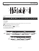

AD5241/AD5242
Rev. C | Page 6 of 20
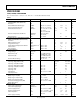
ABSOLUTE MAXIMUM RATINGS
T
A
= 25°C, unless otherwise noted.
Table 3.
Parameter Rating
V
DD
to GND −0.3 V to +7 V
V
SS
to GND 0 V to −7 V
V
DD
to V
SS
7 V
V
A
, V
B
, V
W
to GND V
SS
to V
DD
I
A
, I
B
, I
W
R
AB
= 10 kΩ in TSSOP-14 5.0 mA
1
R
AB
= 100 kΩ in TSSOP-14 1.5 mA
1
R
AB
= 1 MΩ in TSSOP-14 0.5 mA
1
Digital Input Voltage to GND 0 V to V
DD
+ 0.3 V
Operating Temperature Range −40°C to +105°C
Thermal Resistance θ
JA
14-Lead SOIC 158°C/W
16-Lead SOIC 73°C/W
14-Lead TSSOP 206°C/W
16-Lead TSSOP 180°C/W
Maximum Junction Temperature (T
J
max) 150°C
Package Power Dissipation P
D
= (T
J
max − T
A
)/θ
JA
Storage Temperature Range −65°C to +150°C
Lead Temperature
Vapor Phase, 60 sec 215°C
Infrared, 15 sec 220°C
Stresses above those listed under Absolute Maximum Ratings
may cause permanent damage to the device. This is a stress
rating only; functional operation of the device at these or any
other conditions above those indicated in the operational
section of this specification is not implied. Exposure to absolute
maximum rating conditions for extended periods may affect
device reliability.
ESD CAUTION
1
Maximum current increases at lower resistance and different packages.