
Data Sheet

AD5241/AD5242
Rev. C | Page 3 of 20
SPECIFICATIONS
10 kΩ, 100 kΩ, 1 MΩ VERSION
V
DD
= 2.7 V to 5.5 V, V
A
= V
DD
, V
B
= 0 V, −40°C < T
A
< +105°C, unless otherwise noted.
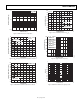
Table 1.
Parameter Symbol Conditions Min Typ
1
Max Unit
DC CHARACTERISTICS, RHEOSTAT MODE
(SPECIFICATIONS APPLY TO ALL VRs)
Resolution N 8 Bits
Resistor Differential Nonlinearity
2
R-DNL R
WB
, V
A
= no connect −1 ±0.4 +1 LSB
Resistor Integral Nonlinearity
2
R-INL R
WB
, V
A
= no connect −2 ±0.5 +2 LSB
Nominal Resistor Tolerance ΔR
AB
/R
AB
T
A
= 25°C, R
AB
= 10 kΩ −30 +30 %
T
A
= 25°C,
R
AB
= 100 kΩ/1 MΩ
−30 +50 %
Resistance Temperature Coefficient
(ΔR
AB
/R
AB
)/
ΔT × 10
6
V
AB
= V
DD
, wiper =
no connect
30 ppm/°C
Wiper Resistance R
W
I
W
= V
DD
/R 60 120 Ω
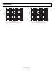
DC CHARACTERISTI
C
S, POTENTIOMETER DIVIDE
R
MODE (SPECIFICATIONS APPLY TO ALL VRs)
Resolution N 8 Bits
Differential Nonlinearity
3
DNL −1 ±0.4 +1 LSB
Integral Nonlinearity
3
INL −2 ±0.5 +2 LSB
Voltage Divider Temperature Coefficient (ΔV
W
/V
W
)/∆T × 10
6
Code = 0x80 5 ppm/°C
Full-Scale Error V
WFSE
Code = 0xFF −1 −0.5 0 LSB
Zero-Scale Error V
WZSE
Code = 0x00 0 0.5 1 LSB
RESISTOR TERMINALS
Voltage Range
4
V
A
, V
B
, V
W
V
SS
V
DD
V
Capacitance (A, B)
5
C
A
, C
B
f = 1 MHz, measured
to GND, code = 0x80
45 pF
Capacitance (W)
5
C
W
f = 1 MHz, measured
to GND, code = 0x80
60 pF
Common-Mode Leakage I
CM
V
A
= V
B
= V
W
1 nA
DIGITAL INPUTS
Input Logic High (SDA and SCL) V
IH
0.7 × V
DD
V
DD
+ 0.5 V V
Input Logic Low (SDA and SCL) V
IL
−0.5 +0.3 × V
DD
V
Input Logic High (AD0 and AD1) V
IH
V
DD
= 5 V 2.4 V
DD
V
Input Logic Low (AD0 and AD1) V
IL
V
DD
= 5 V 0 0.8 V
Input Logic High V
IH
V
DD
= 3 V 2.1 V
DD
V
Input Logic Low V
IL
V
DD
= 3 V 0 0.6 V
Input Current I
IL
V
IH
= 5 V or V
IL
= GND 1 μA
Input Capacitance
5
C
IL
3 pF
DIGITAL OUTPUT
V
OL
I
OL
= 3 mA 0.4 V
Output Logic Low (SDA) V
OL
I
OL
= 6 mA 0.6 V
Output Logic Low (O
1
and O
2
) V
OL
I
SINK
= 1.6 mA 0.4 V
Output Logic High (O
1
and O
2
) V
OH
I
SOURCE
= 40 μA 4 V
Three-State Leakage Current (SDA) I
OZ
V
IH
= 5 V or V
IL
= GND ±1 μA
Output Capacitance
5
C
OZ
3 8 pF
POWER SUPPLIES
Power Single-Supply Range V
DD RANGE
V
SS
= 0 V 2.7 5.5 V
Power Dual-Supply Range V
DD
/V
SS RANGE
±2.3 ±2.7 V
Positive Supply Current I
DD
V
IH
= 5 V or V
IL
= GND 0.1 50 μA
Negative Supply Current I
SS
V
SS
= −2.5 V, V
DD
= +2.5 V +0.1 −50 μA
Power Dissipation
6
P
DISS
V
IH
= 5 V or V
IL
= GND,
V
DD
= 5 V
0.5 250
μW
Power Supply Sensitivity PSS −0.01 +0.002 +0.01 %/%