
Data Sheet

www.austriamicrosystems.com/LED-Driver-ICs/AS1115 Revision 1.08 4 - 25
AS1115
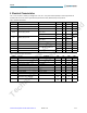
Datasheet - E l e c t rica l C h a racte r i s tics
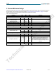
6 Electrical Characteristics
VDD = 2.7V to 5.5V, RSET = 9.53kΩ,
typ. values @
TAMB
= +25ºC,
VDD = 5.0V
(unless otherwise specified). All limits are guaranteed. The
parameters with min and max values are guaranteed with production tests or SQC (Statistical Quality Control) methods.
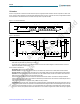
Table 3. Electrical Characteristics
Symbol Parameter Conditions Min Typ Max Unit
TAMB
Operating Temperature Range -4
0 +85 °C
TJ
Operating Junction Temperature Range -40 +125 °C
VDD
Operating Supply Voltage 2.7 5.5 V
IDDSD
Shutdown Supply Current
All digital inputs at VDD or GND,
TAMB = +25ºC
0.2 2 µA
single digit, TAMB = +85ºC 4 µA
IDD
Operating Supply Current
RSET = open circuit.
0.35 0.6
mA
All segments and decimal point on;
ISEG = -40mA.
335
fOSC
Display Scan Rate 8 digits scanned 0.48 0.96 kHz
IDIGIT
Digit Drive Sink Current VOUT = 0.65V 320 mA
ISEG
Segment Drive Source Current
VDD = 5.0V, VOUT = (VDD -1V)
-35 -41 -47 mA
∆ISEG
Segment Drive Current Matching 3 %
ISEG
Segment Drive Source Current Average Current 47 mA
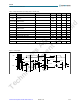
Table 4. Logic Inputs/Outputs Characteristics
Symbol
Parameter
Conditions Min Typ Max Unit
IIH, IIL Input Current SDA, SCL VIN = 0V or VDD -1 1 µ
A
VIH Logic High Input Voltage SDA, SCL 0.7xVDD V
VIL Logic Low Input Voltage SDA, SCL 0.3xVDD V
VOL(SDA) SDA Output Low Voltage ISINK = 3mA 0.4 V
VKEYopen
Keyscan Open Input Voltage 0.8xVDD V
VKEYshort
Keyscan Short Input Voltage 0.7x VDD V
VOL(IRQ) Interrupt Output Low Voltage ISINK = 3mA 0.4 V
∆VI Hysteresis Voltage DIN, CLK, LD/CS 1 V
C
B
Capacitive Load for each Bus Line
550 pF
Open Detection Level Threshold
0.7x
VDD
0.75x
VDD
0.8x
VDD
V
Short Detection Level Threshold
0.05x
VDD
0.1x
VDD
0.15x VDD V
ams AG
Technical content still valid