
Data Sheet

www.austriamicrosystems.com/LED-Driver-ICs/AS1115 Revision 1.08 3 - 25
AS1115
Datasheet - A b s o l ute M a x i m um Rat i n g s
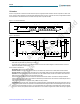
5 Absolute Maximum Ratings
Stresses beyond those listed in Table 2 may cause permanent damage to the device. These are stress ratings only, and functional operation of
the device at these or any other conditions beyond those indicated in Section 6 Electrical Characteristics on page 4 is not implied.
Exposure to absolute maximum rating conditions for extended periods may affect device reliability.
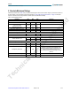
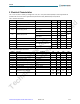
Table 2. Absolute Maximum Ratings
Parameter Min Max Units Comments
Electrical Parameters
VDD to GND -0.3 7 V
All other pins to GND -0.3
7 or
VDD + 0.3
V
DIG0:DIG7 Sink Current 500 mA
SEGA:SEGG, SEGDP Sink Current 100 mA
Input Current (latch-up immunity) -100 100 mA Norm: JEDEC 78
Electrostatic Discharge
Electrostatic Discharge HBM +/- 1 kV Norm: MIL 883 E method 3015
Thermal Information
Thermal Resistance ΘJA
88 °C/W on PCB, QSOP-24 package
30.5 °C/W on PCB, TQFN(4x4)-24 package
Temperature Ranges and Storage Conditions
Junction Temperature +150 ºC
Storage Temperature Range -55 +150 ºC
Package Body Temperature +260 ºC
The reflow peak soldering temperature (body temperature)
specified is in accordance with IPC/JEDEC J-STD-
020“Moisture/Reflow Sensitivity Classification for Non-
Hermetic Solid State Surface Mount Devices”.
The lead finish for Pb-free leaded packages is matte tin
(100% Sn).
Humidity non-condensing 5 85 %
Moisture Sensitive Level 1 Represents a max. floor life time of unlimited
ams AG
Technical content still valid