
Data Sheet

www.austriamicrosystems.com/LED-Driver-ICs/AS1115 Revision 1.08 2 - 25
AS1115
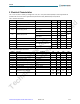
Datasheet - P i n o u t
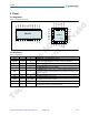
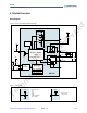
4 Pinout
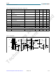
Pin Assignments
Figure 2. Pin Assignments (Top View)
Pin Descriptions
Table 1. Pin Descriptions
Pin Name QSOP-24 TQFN(4x4)-24 Description
SDA
1 22 Serial-Data I/O. Open drain digital I/O I²C data pin.
DIG0:DIG7
2-5, 7-10
1, 2, 4, 5, 6, 7, 23,
24
Digit Drive Lines. Eight digit drive lines that sink current from the display common
cathode. Keyscan detection optional, but must be polled by the µProzessor.
GND
6 3 Ground.
KEYA
11 8 Keyscan Input. Keyscan lines for key readback. Can be used for self-addressing.
KEYB
12 9 Keyscan Input. Keyscan lines for key readback.
ISET
13 10
Set Segment Current. Connect to VDD or a reference voltage through RSET to set the
pe
ak segment current (see Selecting RSET Resistor Value and Using External
Drivers on page 19).
SCL
14 11 Serial-Clock Input. 3.4MHz maximum rate.
IRQ
24 21 Interupt Request Output. Open drain pin.
SEGA:SEGG,
SEGDP
15-18,
20-23
12-15, 17-20
Seven Segment and Decimal Point Drive Lines. 8 seven-segment drives and decimal
point drive that source current to the display.
VDD
19 16 Positive Supply Voltage. Connect to +2.7 to +5.5V supply.
-
Exposed Pad
Exposed Pad. This pin also functions as a heat sink. Solder it to a large pad or to the
circuit-board ground plane to maximize power dissipation.
24
23
22
21
20
19
18
17
16
15
14
13
1
2
3
4
5
6
7
8
9
10
11
12
IRQ
SEGD
SEGDP
SEG E
SEGC
VDD
SEGG
SEGB
SEGF
SEGA
SCL
ISET
SDA
DIG0
DIG1
DIG2
DIG3
GND
DIG4
DIG5
DIG6
DIG7
KEYA
KEYB
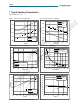
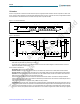
AS1115
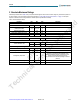
SEG E
KEYA
8
18
SEGB14
DIG2 1
GND 3
AS1115
DIG5 5
ISET
10
SEGA
12
VDD16
SEGC17
SEGG15
SEGF13
DIG3
2
DIG4 4
DIG6
6
SCL
11
KEYB
9
DIG7
7
DIG0
23
IRQ
21
SEGDP
19
SEGD
20
SDA
22
DIG1
24
Exposed
Pad
ams AG
Technical content still valid