austriamicrosystems AG is now ams AG The technical content of this austriamicrosystems datasheet is still valid. Contact information: Headquarters: ams AG Tobelbaderstrasse 30 8141 Unterpremstaetten, Austria Tel: +43 (0) 3136 500 0 e-Mail: ams_sales@ams.com Please visit our website at www.ams.
Datas h eet A S 111 5 64 L E D s, I ²C I n t er f ac ed L E D Dr i v er w i th K ey sc an 2 Key Features 1 General Description up to 1MHz I²C-Compatible Interface Individual LED Segment Control Readback for 16 Keys plus Interrupt Open and Shorted LED Error Detection - Global or Individual Error Detection Hexadecimal- or BCD-Code for 7-Segment Displays 200nA Low-Power Shutdown Current (typ; data retained) Digital and Analog Brightness Control Display Blanked on Power-Up Dri
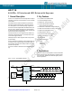
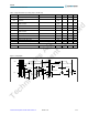
AS1115 Datasheet - P i n o u t 4 Pinout Pin Assignments al id 3 AS1115 DIG5 5 16 VDD 15 SEGG 14 SEGB Exposed Pad 7 8 9 10 11 12 KEYB ISET 13 SEGF KEYA DIG6 6 DIG7 KEYB 12 KEYA 11 DIG7 10 DIG6 9 DIG5 8 SEGDP 17 SEGC GND QSOP-24 1 DIG0:DIG7 2-5, 7-10 GND KEYA KEYB 6 11 12 ISET 13 SCL IRQ SEGA:SEGG, SEGDP 14 24 SCL SEGA am lc s on A te G nt st il GND 6 SEGD DIG3 2 TQFN(4x4)-24 22 Description Serial-Data I/O. Open drain digital I/O I²C data pin.
AS1115 Datasheet - A b s o l u t e M a x i m u m R a t i n g s 5 Absolute Maximum Ratings Stresses beyond those listed in Table 2 may cause permanent damage to the device. These are stress ratings only, and functional operation of the device at these or any other conditions beyond those indicated in Section 6 Electrical Characteristics on page 4 is not implied. Exposure to absolute maximum rating conditions for extended periods may affect device reliability. Table 2.
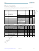
AS1115 Datasheet - E l e c t r i c a l C h a r a c t e r i s t i c s 6 Electrical Characteristics VDD = 2.7V to 5.5V, RSET = 9.53kΩ, typ. values @ TAMB = +25ºC, VDD = 5.0V (unless otherwise specified). All limits are guaranteed. The parameters with min and max values are guaranteed with production tests or SQC (Statistical Quality Control) methods. Table 3.
AS1115 Datasheet - E l e c t r i c a l C h a r a c t e r i s t i c s Table 5.
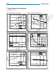
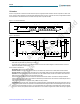
AS1115 Datasheet - Ty p i c a l O p e r a t i n g C h a r a c t e r i s t i c s 7 Typical Operating Characteristics RSET = 9.53kΩ, VRset = VDD; Figure 4. Display Scan Rate vs. Supply Voltage; Figure 5. Display Scan Rate vs. Temperature; 800 780 Vdd=2.7V Vdd=5V Vdd=5.5V 740 720 760 740 lv fosc (Hz) . fosc (Hz) . al id Vdd=4V 780 760 720 700 Tamb=-40°C am lc s on A te G nt st il 700 Tamb=+25°C Tamb=+85°C 680 2.7 3.1 3.5 3.9 4.3 4.7 5.1 680 -40 5.5 -15 10 Figure 6.
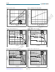
AS1115 Datasheet - Ty p i c a l O p e r a t i n g C h a r a c t e r i s t i c s Figure 10. VDIGIT vs. IDIGIT Figure 11. Input High Level vs. Supply Voltage 0.4 3.5 3 2.5 0.2 1.5 1 = 2.7V = 3.3V = 4V = 5V = 5.5V 0.5 0 0 0.05 0.1 0.15 0.2 Idig (A) 0.25 0.3 Figure 12. ISEG vs. VSEG; VDD = 5V 50 40 3.5 4.3 4.7 5.1 5.5 Vdd (V) 50 = 10k = 13k = 18k = 30k = 56k Rext Rext Rext Rext Rext 45 40 = 8k2 = 10k = 13k = 18k = 30k Iseg (mA) .
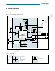
AS1115 Datasheet - D e t a i l e d D e s c r i p t i o n 8 Detailed Description Block Diagram al id Figure 16. AS1115 - Block Diagram (QSOP-24 Package) Open/Short Detection + – RSET 19 + am lc s on A te G nt st il VDD – Oszillator VDD lv VDD 13 ISET 24 IRQ 8 SEGA-G, SEGDP Digital Control Logic 8 2-5, 7-10 DIG0 to DIG7 (PWM, Debounce,....
AS1115 Datasheet - D e t a i l e d D e s c r i p t i o n I²C Interface The AS1115 supports the I²C serial bus and data transmission protocol in high-speed mode at 3.4MHz. The AS1115 operates as a slave on the I²C bus. The bus must be controlled by a master device that generates the serial clock (SCL), controls the bus access, and generates the START and STOP conditions. Connections to the bus are made via the open-drain I/O pins SCL and SDA.
AS1115 Datasheet - D e t a i l e d D e s c r i p t i o n al id ing an acknowledge bit on the last byte that has been clocked out of the slave. In this case, the slave must leave the data line HIGH to enable the master to generate the STOP condition. - Figure 19 on page 9 details how data transfer is accomplished on the I²C bus. Depending upon the state of the R/W bit, two types of data transfer are possible: - Master Transmitter to Slave Receiver.
AS1115 Datasheet - D e t a i l e d D e s c r i p t i o n Command Byte The AS1115 operation, (see Table 6) is determined by a command byte (see Figure 21 on page 11). Figure 21. Command Byte 6 5 4 3 2 1 LSB D15 D14 D13 D12 D11 D10 D09 D08 al id MSB Figure 22.
AS1115 Datasheet - D e t a i l e d D e s c r i p t i o n Initial Power-Up On initial power-up, the AS1115 registers are reset to their default values, the display is blanked, and the device goes into shutdown mode. At this time, all registers should be programmed for normal operation. Note: The default settings enable only scanning of one digit; the internal decoder is disabled and the Intensity Control Register (see page 17) is set to the minimum values.
AS1115 Datasheet - D e t a i l e d D e s c r i p t i o n Address Register Page D12 D11 D10 D9 D8 Diagnostic Digit 0 000 1 0 1 0 0 N/A Diagnostic Digit 1 000 1 0 1 0 1 N/A Diagnostic Digit 2 000 1 0 1 1 0 N/A Diagnostic Digit 3 000 1 0 1 1 1 N/A Diagnostic Digit 4 000 1 1 0 0 0 Diagnostic Digit 5 000 1 1 0 0 1 Diagnostic Digit 6 000 1 1 0 1 0 Diagnostic Digit 7 000 1 1 0 1 1 KEYA 000 1 1 1 0 0 KEYB 000 1 1 1 0 1 D7:D0 al id
AS1115 Datasheet - D e t a i l e d D e s c r i p t i o n Figure 25. Standard 7-Segment LED Intensity Control and Inter-Digit Blanking A F B G E DP Table 9.
AS1115 Datasheet - D e t a i l e d D e s c r i p t i o n Table 11. No-Decode Mode Data Bits and Corresponding Segment Lines D7 DP Corresponding Segment Line D6 A D5 B D4 C D3 D D2 E D1 F D0 G I²C Self Addressing al id If this feature is used, 2 of the 16 key readback nodes can be left open or shorted for self-addressing. This is done with KEYA together with SEGG (A0) and SEGF (A1). This two nodes cannot be used for key-readback in this case.
AS1115 Datasheet - D e t a i l e d D e s c r i p t i o n Display-Test Mode The AS1115 can detect open or shorted LEDs. Readout of either open LEDs or short LEDs is possible, as well as a OR relation of open and short. Note: All settings of the digit- and control-registers are maintained. Table 14. Testmode Register Summary D6 RSET_short D5 RSET_open D4 LED_global D3 LED_test D2 LED_open D1 LED_short D0 DISP_test al id D7 X Table 15.
AS1115 Datasheet - D e t a i l e d D e s c r i p t i o n Display brightness is controlled by an integrated pulse-width modulator which is controlled by the lower-nibble of the Intensity Control Register. The modulator scales the average segment-current in 16 steps from a maximum of 15/16 down to 1/16 of the peak current set by RSET. Table 17.
AS1115 Datasheet - D e t a i l e d D e s c r i p t i o n Feature Register (0x0E) The Feature Register is used for enabling various features including switching the device into external clock mode, applying an external reset, selecting code-B or HEX decoding, enabling or disabling blinking, setting the blinking rate, and resetting the blink timing. Note: At power-up the Feature Register is initialized to 0. Table 20.
AS1115 Datasheet - Ty p i c a l A p p l i c a t i o n 9 Typical Application Selecting RSET Resistor Value and Using External Drivers Brightness of the display segments is controlled via RSET. The current that flows into ISET defines the current that flows through the LEDs. al id Segment current is about 200 times the current in ISET. Typical values for RSET for different segment currents, operating voltages, and LED voltage drop (VLED) are given in Table 22 & Table 23.
AS1115 Datasheet - Ty p i c a l A p p l i c a t i o n 8x8 Dot Matrix Mode The application example in Figure 27 shows the AS1115 in the 8x8 LED dot matrix mode. The LED columns have common cathodes and are connected to the DIG0:7 outputs. The rows are connected to the segment drivers. Each of the 64 LEDs can be addressed separately. The columns are selected via the digits as listed in Table 6 on page 12.
AS1115 Datasheet - P a c k a g e D r a w i n g s a n d M a r k i n g s 10 Package Drawings and Markings am lc s on A te G nt st il lv al id Figure 29. QSOP-24 Marking Figure 30. TQFN(4x4)-24 Marking Table 24. Packaging Code YY WW manufacturing week R/X ZZ plant identifier free choice / traceability code Te ch ni ca last two digits of the current year www.austriamicrosystems.com/LED-Driver-ICs/AS1115 Revision 1.
AS1115 Datasheet - P a c k a g e D r a w i n g s a n d M a r k i n g s Te ch ni ca am lc s on A te G nt st il lv al id Figure 31. QSOP-24 Package www.austriamicrosystems.com/LED-Driver-ICs/AS1115 Revision 1.
AS1115 Datasheet - P a c k a g e D r a w i n g s a n d M a r k i n g s Te ch ni ca am lc s on A te G nt st il lv al id Figure 32. TQFN(4x4)-24 Package www.austriamicrosystems.com/LED-Driver-ICs/AS1115 Revision 1.
AS1115 Datasheet - O r d e r i n g I n f o r m a t i o n 11 Ordering Information The devices are available as the standard products shown in Table 25. Table 25. Ordering Information Description 64 LEDs, I²C Interfaced LED Driver with Keyscan Delivery Form Tape and Reel Tape and Reel Note: All products are RoHS compliant and austriamicrosystems green. Buy our products or get free samples online at ICdirect: http://www.austriamicrosystems.com/ICdirect Technical Support is found at http://www.
AS1115 Datasheet Copyrights Copyright © 1997-2012, austriamicrosystems AG, Tobelbaderstrasse 30, 8141 Unterpremstaetten, Austria-Europe. Trademarks Registered ®. All rights reserved. The material herein may not be reproduced, adapted, merged, translated, stored, or used without the prior written consent of the copyright owner. All products and companies mentioned are trademarks or registered trademarks of their respective companies.