
Data Sheet

© 2009 Microchip Technology Inc. DS22226A-page 27
MCP3426/7/8
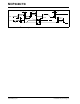
High Speed Mode (3.4 MHz)
Clock frequency f
SCL
0—3.4MHzC
b
= 100 pF
0—1.7MHzC
b
= 400 pF
Clock high time
T
HIGH
60 — — ns C
b
= 100 pF, f
SCL
= 3.4 MHz
120 — — ns C
b
= 400 pF, f
SCL
= 1.7 MHz
Clock low time
T
LOW
160 — — ns C
b
= 100 pF, f
SCL
= 3.4 MHz
320 — — ns C
b
= 400 pF, f
SCL
= 1.7 MHz
SCL rise time
(Note 1)
T
R
— — 40 ns From V
IL
to V
IH
,
C
b
= 100 pF, f
SCL
= 3.4 MHz
— — 80 ns From V
IL
to V
IH
,
C
b
= 400 pF, f
SCL
= 1.7 MHz
SCL fall time
(Note 1)
T
F
— — 40 ns From V
IH
to V
IL
,
C
b
= 100 pF, f
SCL
= 3.4 MHz
— — 80 ns From V
IH
to V
IL
,
C
b
= 400 pF, f
SCL
= 1.7 MHz
SDA rise time
(Note 1)
T
R: DAT
— — 80 ns From V
IL
to V
IH
,
C
b
= 100 pF, f
SCL
= 3.4 MHz
— — 160 ns From V
IL
to V
IH
,
C
b
= 400 pF, f
SCL
= 1.7 MHz
SDA fall time
(Note 1)
T
F: DATA
— — 80 ns From V
IH
to V
IL
,
C
b
= 100 pF, f
SCL
= 3.4 MHz
— — 160 ns From V
IH
to V
IL
,
C
b
= 400 pF, f
SCL
= 1.7 MHz
Data hold time
(Note 4)
T
HD:DAT
0 — 70 ns C
b
= 100 pF, f
SCL
= 3.4 MHz
0 — 150 ns C
b
= 400 pF, f
SCL
= 1.7 MHz
Output valid from clock
(Notes 2 and 3)
T
AA
— — 150 ns C
b
= 100 pF, f
SCL
= 3.4 MHz
— — 310 ns C
b
= 400 pF, f
SCL
= 1.7 MHz
START condition hold time
T
HD:STA
160 — — ns After this period, the first clock
pulse is generated
Repeated START condition
setup time
T
SU:STA
160 — — ns Only relevant for repeated Start
condition
Data input setup time
T
SU:DAT
10 — — ns
STOP condition setup time
T
SU:STO
160 — — ns
Input filter spike suppression
T
SP
0 — 10 ns SDA and SCL pins (Note 5)
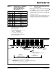
TABLE 5-5: I
2
C SERIAL TIMING SPECIFICATIONS (CONTINUED)
Electrical Specifications: Unless otherwise specified, all limits are specified for T
A
= -40 to +85°C, V
DD
= +2.7V to +5.0V,
V
SS
= 0V, CHn+ = CHn- = V
REF
/2.
Parameters Sym Min Typ Max Units Conditions
Note 1: This parameter is ensured by characterization and not 100% tested.
2: This specification is not a part of the I
2
C specification. This specification is equivalent to the Data Hold Time (T
HD:DAT
)
plus SDA Fall (or rise) time:
T
AA
= T
HD:DAT
+ T
F
(OR T
R
).
3: If this parameter is too short, it can create an unintended Start or Stop condition to other devices on the bus line. If this
parameter is too long, Clock Low time (T
LOW
) can be affected.
4: For Data Input: This parameter must be longer than t
SP
. If this parameter is too long, the Data Input Setup (T
SU:DAT
) or
Clock Low time (T
LOW
) can be affected.
For Data Output: This parameter is characterized, and tested indirectly by testing T
AA
parameter.
5: This parameter is ensured by characterization and not 100% tested. This parameter is not available for Standard Mode.