
Data Sheet


MCP3426/7/8
DS22226A-page 2 © 2009 Microchip Technology Inc.
The I
2
C address bits for the MCP3427 and MCP3428
are selected by using two external I
2
C address
selection pins (Adr0 and Adr1). The user can configure
the device to one of eight available addresses by
connecting these two address selection pins to V
DD
,
V
SS
or float. The I
2
C address bits of the MCP3426 are
programmed at the factory during production.
The MCP3426 is available in 8-pin SOIC, DFN, and
MSOP packages. The MCP3427 is available in 10-pin
DFN, and MSOP packages. The MCP3428 is available
in 14-pin SOIC and TSSOP packages.
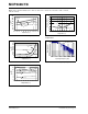
Package Types
MCP3426
Functional Block Diagram
4
5
6
9
CH2-
V
SS
CH3+
Adr1
Adr0
3
12
CH2+
CH3-
2
13
CH1-
CH4+
1
14
CH1+
CH4-
7
8
SDA
SCL
V
DD
MCP3428
11
10
SOIC, TSSOP
2
3
4
7
8
9
CH1-
V
DD
SDA
Adr0
V
SS
SCL
1
10
CH1+
Adr1
5
6
CH2-
CH2+
MCP3427
2
3
4
5
6
7
CH1-
V
DD
SDA
CH2+
V
SS
SCL
1
8
CH1+
CH2-
MCP3426
MSOP, SOIC MSOP
MCP3426
2x3 DFN *
V
DD
CH1-
SDA
CH2+
V
SS
1
2
3
4
8
7
6
5
SCL
CH2-CH1+
* Includes Exposed Thermal Pad (EP); see Table 3-1.
EP
9
MCP3427
3x3 DFN *
V
SS
CH1-
CH2+
Adr0
SCL
1
2
3
4
10
9
8
7
SDA
Adr1CH1+
EP
11
CH2-
5 6
V
DD
V
SS
V
DD
PGA
SCL
SDA
MUX
I
2
C
Interface
Gain = 1, 2, 4, or 8
Voltage Reference
Clock
(2.048V)
V
REF
ΔΣ ADC
Converter
Oscillator
MCP3426
CH1+
CH1-
CH2+
CH2-