
Data Sheet

MCP3426/7/8
DS22226A-page 12 © 2009 Microchip Technology Inc.
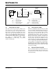
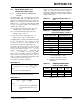
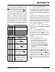
FIGURE 3-1: Equivalent Analog Input Circuit.
3.3 Serial Clock Pin (SCL)
SCL is the serial clock pin of the I
2
C interface. The
device acts only as a slave and the SCL pin accepts
only external serial clocks. The input data from the
Master device is shifted into the SDA pin on the rising
edges of the SCL clock and output from the slave
device occurs at the falling edges of the SCL clock. The
SCL pin is an open-drain N-channel driver. Therefore,
it needs a pull-up resistor from the V
DD
line to the SCL
pin. Refer to Section 5.3 “I
2
C Serial
Communications” for more details on I
2
C Serial
Interface communication.
3.4 Serial Data Pin (SDA)
SDA is the serial data pin of the I
2
C interface. The SDA
pin is used for input and output data. In read mode, the
conversion result is read from the SDA pin (output). In
write mode, the device configuration bits are written
(input) though the SDA pin. The SDA pin is an
open-drain N-channel driver. Therefore, it needs a
pull-up resistor from the V
DD
line to the SDA pin.
Except for start and stop conditions, the data on the
SDA pin must be stable during the high period of the
clock. The high or low state of the SDA pin can only
change when the clock signal on the SCL pin is low.
Refer to Section 5.3 “I
2
C Serial Communications”
for more details on I
2
C Serial Interface communication.
The typical range of the pull-up resistor value for SCL
and SDA is from 5 kΩ to 10 kΩ for standard (100 kHz)
and fast (400 kHz) modes, and less than 1 kΩ for high
speed mode (3.4 MHz).
3.5 Exposed Thermal Pad (EP)
There is an internal electrical connection between the
Exposed Thermal Pad (EP) and the V
SS
pin; they must
be connected to the same potential on the Printed
Circuit Board (PCB).
C
PIN
V
R
SS
CHn
4pF
V
T
= 0.6V
V
T
= 0.6V
I
LEAKAGE
Sampling
Switch
SS
R
S
C
SAMPLE
(3.2 pF)
V
DD
(~ ±1 nA)
LEGEND
V = Signal Source I
LEAKAGE
= Leakage Current at Analog Pin
R
ss
= Source Impedance SS = Sampling Switch
CHn = Analog Input Pin R
s
= Sampling Switch Resistor
C
PIN
= Input Pin Capacitance C
SAMPLE
= Sample Capacitance
V
T
= Threshold Voltage D1, D2 = ESD Protection Diode
D
1
D
2
V
SS