
Data Sheet
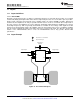


Time (us)
Current (I), Voltage (V)
0 2 4 6 8 10 12 14 16 18 20
-10
-7.5
-5
-2.5
0
2.5
5
7.5
10
I_in
VOUT
INA193
,
INA194
,
INA195
INA196
,
INA197
,
INA198
www.ti.com
SBOS307G –MAY 2004–REVISED JANUARY 2015
Typical Application (continued)
9.2.2 Detailed Design Procedure
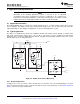
The ability to measure this current flowing in both directions is enabled by adding a unity gain amplifier with a
V
REF
, as shown in Figure 29. The output then responds by increasing above VREF for positive differential signals
(relative to the IN – pin) and responds by decreasing below VREF for negative differential signals. This reference
voltage applied to the REF pin can be set anywhere between 0 V to V+. For bidirectional applications, VREF is
typically set at mid- scale for equal signal range in both current directions. In some cases, however, VREF is set
at a voltage other than mid-scale when the bidirectional current and corresponding output signal do not need to
be symmetrical.
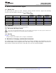
9.2.3 Application Curve
An example output response of a bidirectional configuration is shown in Figure 30. With the REF pin connected
to a reference voltage, 2.5 V in this case, the output voltage is biased upwards by this reference level. The
output rises above the reference voltage for positive differential input signals and falls below the reference
voltage for negative differential input signals.
Figure 30. Output Voltage vs Shunt Input Current
10 Power Supply Recommendations
The input circuitry of the INA193-INA198 devices can accurately measure beyond its power-supply voltage, V+.
For example, the V+ power supply can be 5 V, whereas the load power-supply voltage is up to 80 V. The output
voltage range of the OUT terminal, however, is limited by the voltages on the power-supply pin.
Copyright © 2004–2015, Texas Instruments Incorporated Submit Documentation Feedback 23
Product Folder Links: INA193 INA194 INA195 INA196 INA197 INA198