
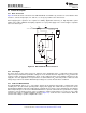
Data Sheet

R
S
A1
0.1 Fm
V+>3V
A2
R
L
Load
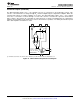
V
IN+
-16Vto+80V
Negative
and
Positive
Common-Mode
Voltage
V
IN+
V
IN-
V+
I
L
OUT
INA193-INA198
R
1
R
2
2.4
2.2
2.0
1.8
1.6
1.4
1.2
1.0
0.8
0.6
0.4
0.2
0
0
2
4 6 8
10 12 14 16 18 20 22
V (V)
OUT
V (mV)
SENSE
24
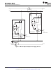
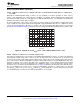
INA195,INA198V TestedLimit
OUT
(1)
V
CM2
V
CM3
V
CM4
V ,V ,andV
CM2 CM3 CM4
illustratethevariance
fromparttopartoftheV thatcancause
CM
maximumV
OUT SENSE
withV <20mV.
V testedlimitat
OUT
V =0mV,0 V£
SENSE CM1 S
V£ .
Ideal
VCM1
INA193
,
INA194
,
INA195
INA196
,
INA197
,
INA198
SBOS307G –MAY 2004–REVISED JANUARY 2015
www.ti.com
Device Functional Modes (continued)
(1) INA193, INA196 V
OUT
Tested Limit = 0.4V. INA194, INA197 V
OUT
Tested Limit = 1V.
Figure 27. Example for Low V
SENSE
Case 2 (INA195, INA198: Gain = 100)
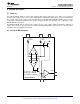
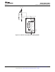
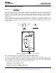
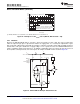
8.4.3 Shutdown
Because the INA193-INA198 devices consume a quiescent current less than 1 mA, they can be powered by
either the output of logic gates or by transistor switches to supply power. Use a totem-pole output buffer or gate
that can provide sufficient drive along with 0.1-μF bypass capacitor, preferably ceramic with good high-frequency
characteristics. This gate should have a supply voltage of 3 V or greater because the INA193-INA198 devices
require a minimum supply greater than 2.7 V. In addition to eliminating quiescent current, this gate also turns off
the 10-μA bias current present at each of the inputs. An example shutdown circuit is shown in Figure 28.
Figure 28. INA193-INA198 Example Shutdown Circuit
20 Submit Documentation Feedback Copyright © 2004–2015, Texas Instruments Incorporated
Product Folder Links: INA193 INA194 INA195 INA196 INA197 INA198