
Data Sheet
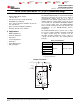

INA193
,
INA194
,
INA195
INA196
,
INA197
,
INA198
SBOS307G –MAY 2004–REVISED JANUARY 2015
www.ti.com
Table of Contents
8.3 Feature Description................................................. 12
1 Features.................................................................. 1
8.4 Device Functional Modes........................................ 16
2 Applications ........................................................... 1
9 Application and Implementation ........................ 22
3 Description ............................................................. 1
9.1 Application Information............................................ 22
4 Revision History..................................................... 2
9.2 Typical Application .................................................. 22
5 Device Comparison Table..................................... 3
10 Power Supply Recommendations ..................... 23
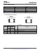
6 Pin Configuration and Functions......................... 3
11 Layout................................................................... 24
7 Specifications......................................................... 4
11.1 Layout Guidelines ................................................. 24
7.1 Absolute Maximum Ratings ...................................... 4
11.2 Layout Example .................................................... 24
7.2 ESD Ratings ............................................................ 4
12 Device and Documentation Support ................. 25
7.3 Recommended Operating Conditions....................... 4
12.1 Related Links ........................................................ 25
7.4 Thermal Information.................................................. 4
12.2 Trademarks........................................................... 25
7.5 Electrical Characteristics........................................... 5
12.3 Electrostatic Discharge Caution............................ 25
7.6 Typical Characteristics.............................................. 7
12.4 Glossary................................................................ 25
8 Detailed Description ............................................ 11
13 Mechanical, Packaging, and Orderable
8.1 Overview ................................................................. 11
Information ........................................................... 25
8.2 Functional Block Diagram ....................................... 11
4 Revision History
NOTE: Page numbers for previous revisions may differ from page numbers in the current version.
Changes from Revision F (February 2010) to Revision G Page
• Added ESD Ratings table, Feature Description section, Device Functional Modes, Application and Implementation
section, Power Supply Recommendations section, Layout section, Device and Documentation Support section, and
Mechanical, Packaging, and Orderable Information section ................................................................................................. 4
Changes from Revision E (August 2006) to Revision F Page
• Updated document format to current standards..................................................................................................................... 1
• Added test conditions to Output, Total Output Error parameter in Electrical Characteristics: V
S
= +12V.............................. 5
2 Submit Documentation Feedback Copyright © 2004–2015, Texas Instruments Incorporated
Product Folder Links: INA193 INA194 INA195 INA196 INA197 INA198