
Data Sheet

2.0
1.8
1.6
1.4
1.2
1.0
0.8
0.6
0.4
0.2
0
0
2
4 6 8
10 12 14 16 18
V (V)
OUT
V (mV)
SENSE
20
Actual
Ideal
INA193
,
INA194
,
INA195
INA196
,
INA197
,
INA198
www.ti.com
SBOS307G –MAY 2004–REVISED JANUARY 2015
Device Functional Modes (continued)
8.4.2.3 Low V
SENSE
Case 1: V
SENSE
< 20mV, −16v ≤ V
CM
< 0; and Low V
SENSE
Case 3: V
SENSE
< 20mV, V
S
<
V
CM
≤ 80V
Although the INA193−INA198 family of devices are not designed for accurate operation in either of these
regions, some applications are exposed to these conditions; for example, when monitoring power supplies that
are switched on and off while V
S
is still applied to the INA193−INA198 devices. It is important to know what the
behavior of the devices will be in these regions.
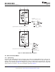
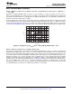
As V
SENSE
approaches 0 mV, in these V
CM
regions, the device output accuracy degrades. A larger-than-normal
offset can appear at the current shunt monitor output with a typical maximum value of V
OUT
= 300 mV for V
SENSE
= 0 mV. As V
SENSE
approaches 20 mV, V
OUT
returns to the expected output value with accuracy as specified in
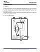
the Electrical Characteristics. Figure 26 illustrates this effect using the INA195 and INA198 devices (Gain = 100).
Figure 26. Example for Low V
SENSE
Cases 1 and 3 (INA195, INA198: Gain = 100)
8.4.2.4 Low V
SENSE
Case 2: V
SENSE
< 20 mV, 0 V ≤ V
CM
≤ V
S
This region of operation is the least accurate for the INA193−INA198 family of devices. To achieve the wide input
common-mode voltage range, these devices use two op amp front ends in parallel. One op amp front end
operates in the positive input common-mode voltage range, and the other in the negative input region. For this
case, neither of these two internal amplifiers dominates and overall loop gain is very low. Within this region, V
OUT
approaches voltages close to linear operation levels for Normal Case 2. This deviation from linear operation
becomes greatest the closer V
SENSE
approaches 0 V. Within this region, as V
SENSE
approaches 20 mV, device
operation is closer to that described by Normal Case 2. Figure 27 illustrates this behavior for the INA195 device.
The V
OUT
maximum peak for this case is tested by maintaining a constant V
S
, setting V
SENSE
= 0 mV and
sweeping V
CM
from 0 V to V
S
. The exact V
CM
at which V
OUT
peaks during this test varies from part to part, but the
V
OUT
maximum peak is tested to be less than the specified V
OUT
Tested Limit.
Copyright © 2004–2015, Texas Instruments Incorporated Submit Documentation Feedback 19
Product Folder Links: INA193 INA194 INA195 INA196 INA197 INA198