
Data Sheet

V RTI(Referred-To-Input)=
OS
V
OUT1
G
- 100mV
G=
V V
OUT1 OUT2
-
100mV 20mV-
INA193
,
INA194
,
INA195
INA196
,
INA197
,
INA198
SBOS307G –MAY 2004–REVISED JANUARY 2015
www.ti.com
Device Functional Modes (continued)
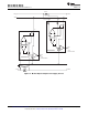
Low V
SENSE
Case 3: V
SENSE
< 20mV, V
S
< V
CM
≤ 80V
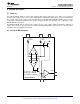
8.4.2.1 Normal Case 1: V
SENSE
≥ 20mv, V
CM
≥ V
S
This region of operation provides the highest accuracy. Here, the input offset voltage is characterized and
measured using a two-step method. First, the gain is determined by Equation 2.
where:
V
OUT1
= Output Voltage with V
SENSE
= 100mV
V
OUT2
= Output Voltage with V
SENSE
= 20mV (2)
Then the offset voltage is measured at V
SENSE
= 100mV and referred to the input (RTI) of the current shunt
monitor, as shown in Equation 3.
(3)
In the Typical Characteristics, the Output Error vs Common-Mode Voltage curve (Figure 6) shows the highest
accuracy for this region of operation. In this plot, V
S
= 12 V; for V
CM
≥ 12 V, the output error is at its minimum.
This case is also used to create the V
SENSE
≥ 20-mV output specifications in the Electrical Characteristics table.
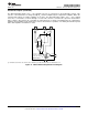
8.4.2.2 Normal Case 2: V
SENSE
≥ 20mv, V
CM
< V
S
This region of operation has slightly less accuracy than Normal Case 1 as a result of the common-mode
operating area in which the part functions, as seen in the Output Error vs Common-Mode Voltage curve
(Figure 6). As noted, for this graph V
S
= 12 V; for V
CM
< 12 V, the Output Error increases as V
CM
becomes less
than 12 V, with a typical maximum error of 0.005% at the most negative V
CM
= −16V.
18 Submit Documentation Feedback Copyright © 2004–2015, Texas Instruments Incorporated
Product Folder Links: INA193 INA194 INA195 INA196 INA197 INA198