
Data Sheet
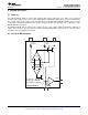
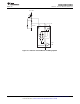

R
1
R
2 REF
1.25V
Internal
Reference
Foroutput
signals>comparatortrip-point.
(a) INA193-INA198outputadjustedbyvoltagedivider.
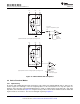
TLV3012
REF
1.25V
Internal
Reference
R
1
R
2
Forusewith
smalloutputsignals.
(b) Comparatorreferencevoltageadjustedbyvoltagedivider.
TLV3012
OUT
V
IN+
V
IN-
V+
INA193-INA198
OUT
V
IN+
V
IN-
V+
INA193-INA198
INA193
,
INA194
,
INA195
INA196
,
INA197
,
INA198
SBOS307G –MAY 2004–REVISED JANUARY 2015
www.ti.com
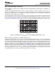
Figure 24. INA193-INA198 with Comparator
8.4 Device Functional Modes
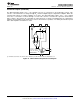
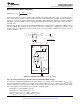
8.4.1 Input Filtering
An obvious and straightforward location for filtering is at the output of the INA193-INA198 devices; however, this
location negates the advantage of the low output impedance of the internal buffer. The only other option for
filtering is at the input pins of the INA193-INA198 devices, which is complicated by the internal 5-kΩ + 30% input
impedance; this is illustrated in Figure 25. Using the lowest possible resistor values minimizes both the initial shift
in gain and effects of tolerance. The effect on initial gain is given by Equation 1:
16 Submit Documentation Feedback Copyright © 2004–2015, Texas Instruments Incorporated
Product Folder Links: INA193 INA194 INA195 INA196 INA197 INA198