
Data Sheet
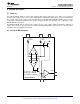
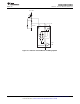

A1
A2
R
L
(1)
V
IN+
V
IN
V+
OUT
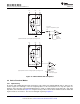
INA193-INA198
R
1
(1)
5 k:
G = 20, R
L
= 100 k:
G = 50, R
L
= 250 k:
G = 100, R
L
= 500 k:
R
1
(1)
5 k:
GND
INA193
,
INA194
,
INA195
INA196
,
INA197
,
INA198
www.ti.com
SBOS307G –MAY 2004–REVISED JANUARY 2015
Feature Description (continued)
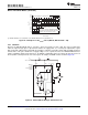
The differential input voltage, (V
IN+
) − (V
IN−
) applied across R
S
, is converted to a current through a resistor. This
current is converted back to a voltage through R
L
, and then amplified by the output buffer amplifier. When the
common-mode voltage is negative, amplifier A1 is active. The differential input voltage, (V
IN+
) − (V
IN−
) applied
across R
S
, is converted to a current through a resistor. This current is sourced from a precision current mirror
whose output is directed into R
L
converting the signal back into a voltage and amplified by the output buffer
amplifier. Patent-pending circuit architecture ensures smooth device operation, even during the transition period
where both amplifiers A1 and A2 are active.
(1) Nominal resistor values are shown. ±15% variation is possible. Resistor ratios are matched to ± 1%.
Figure 21. INA193-INA198 Simplified Circuit Diagram
Copyright © 2004–2015, Texas Instruments Incorporated Submit Documentation Feedback 13
Product Folder Links: INA193 INA194 INA195 INA196 INA197 INA198