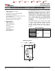
Product Folder Sample & Buy Support & Community Tools & Software Technical Documents Reference Design INA193, INA194, INA195 INA196, INA197, INA198 SBOS307G – MAY 2004 – REVISED JANUARY 2015 INA19x Current Shunt Monitor −16 V to +80 V Common-Mode Range 1 Features 3 Description • The INA193−INA198 family of current shunt monitors with voltage output can sense drops across shunts at common-mode voltages from −16 V to +80 V, independent of the INA19x supply voltage.
INA193, INA194, INA195 INA196, INA197, INA198 SBOS307G – MAY 2004 – REVISED JANUARY 2015 www.ti.com Table of Contents 1 2 3 4 5 6 7 8 Features .................................................................. Applications ........................................................... Description ............................................................. Revision History..................................................... Device Comparison Table.....................................
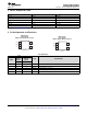
INA193, INA194, INA195 INA196, INA197, INA198 www.ti.com SBOS307G – MAY 2004 – REVISED JANUARY 2015 5 Device Comparison Table PART NUMBER GAIN PINOUT(1) INA193 20 V/V Pinout #1 INA194 50 V/V Pinout #1 INA195 100 V/V Pinout #1 INA196 20 V/V Pinout #2 INA197 50 V/V Pinout #2 INA198 100 V/V Pinout #2 (1) See Pin Configuration and Functions for Pinout #1 and Pinout #2.
INA193, INA194, INA195 INA196, INA197, INA198 SBOS307G – MAY 2004 – REVISED JANUARY 2015 www.ti.com 7 Specifications 7.1 Absolute Maximum Ratings over operating free-air temperature range (unless otherwise noted) (1) MIN MAX UNIT 18 V Supply Voltage Analog Inputs, VIN+, VIN− –18 18 V Differential (VIN+) – (VIN−) –18 18 V Common-Mode (2) –16 80 V GND – 0.3 (V+) + 0.
INA193, INA194, INA195 INA196, INA197, INA198 www.ti.com SBOS307G – MAY 2004 – REVISED JANUARY 2015 7.5 Electrical Characteristics All specifications at TA = 25°C, VS = 12 V, VIN+ = 12 V, and VSENSE = 100 mV, unless otherwise noted. PARAMETER TEST CONDITIONS TA = −40°C to +125°C TA = 25°C MIN TYP MAX UNIT TYP MAX MIN 0.15 (VS – 0.
INA193, INA194, INA195 INA196, INA197, INA198 SBOS307G – MAY 2004 – REVISED JANUARY 2015 www.ti.com Electrical Characteristics (continued) All specifications at TA = 25°C, VS = 12 V, VIN+ = 12 V, and VSENSE = 100 mV, unless otherwise noted.
INA193, INA194, INA195 INA196, INA197, INA198 www.ti.com SBOS307G – MAY 2004 – REVISED JANUARY 2015 7.6 Typical Characteristics All specifications at TA = 25°C, VS = 12 V, and VIN+ = 12 V, and VSENSE = 100 mV, unless otherwise noted. 45 40 G = 50 35 Gain (dB) 30 G = 100 40 G = 50 35 Gain (dB) 45 CLOAD = 1000pF G = 100 G = 20 25 20 30 20 15 15 10 10 5 G = 20 25 5 10k 100k 10k 1M 100k Frequency (Hz) Figure 1. Gain vs Frequency Figure 2.
INA193, INA194, INA195 INA196, INA197, INA198 SBOS307G – MAY 2004 – REVISED JANUARY 2015 www.ti.com Typical Characteristics (continued) All specifications at TA = 25°C, VS = 12 V, and VIN+ = 12 V, and VSENSE = 100 mV, unless otherwise noted. 12 1000 11 10 Sourcing Current 9 800 +25°C 8 700 -40°C +125°C 7 6 VS = 3V 5 Sourcing Current +25°C 4 -40°C 2 +125°C 0 400 300 200 100 0 5 0 500 Output stage is designed to source current. Current sinking capability is approximately 400mA.
INA193, INA194, INA195 INA196, INA197, INA198 www.ti.com SBOS307G – MAY 2004 – REVISED JANUARY 2015 Typical Characteristics (continued) All specifications at TA = 25°C, VS = 12 V, and VIN+ = 12 V, and VSENSE = 100 mV, unless otherwise noted. G = 20 Output Voltage (50mV/div) Output Voltage (500mV/div) G = 20 VSENSE = 10mV to 20mV VSENSE = 10mV to 100mV Time (2ms/div) Time (2ms/div) Figure 13. Step Response Figure 14.
INA193, INA194, INA195 INA196, INA197, INA198 SBOS307G – MAY 2004 – REVISED JANUARY 2015 www.ti.com Typical Characteristics (continued) All specifications at TA = 25°C, VS = 12 V, and VIN+ = 12 V, and VSENSE = 100 mV, unless otherwise noted. Output Voltage (2V/div) G = 100 VSENSE = 10mV to 100mV Time (10ms/div) Figure 19.
INA193, INA194, INA195 INA196, INA197, INA198 www.ti.com SBOS307G – MAY 2004 – REVISED JANUARY 2015 8 Detailed Description 8.1 Overview The INA193−INA198 family of current shunt monitors with voltage output can sense drops across shunts at common-mode voltages from −16 V to +80 V, independent of the INA19x supply voltage. They are available with three output voltage scales: 20 V/V, 50 V/V, and 100 V/V. The 500-kHz bandwidth simplifies use in current control loops.
INA193, INA194, INA195 INA196, INA197, INA198 SBOS307G – MAY 2004 – REVISED JANUARY 2015 www.ti.com 8.3 Feature Description 8.3.1 Basic Connection Figure 20 shows the basic connection of the INA193-INA198. To minimize any resistance in series with the shunt resistance, connect the input pins, VIN+ and VIN−, as closely as possible to the shunt resistor. Power-supply bypass capacitors are required for stability.
INA193, INA194, INA195 INA196, INA197, INA198 www.ti.com SBOS307G – MAY 2004 – REVISED JANUARY 2015 Feature Description (continued) The differential input voltage, (VIN+) − (VIN−) applied across RS, is converted to a current through a resistor. This current is converted back to a voltage through RL, and then amplified by the output buffer amplifier. When the common-mode voltage is negative, amplifier A1 is active.
INA193, INA194, INA195 INA196, INA197, INA198 SBOS307G – MAY 2004 – REVISED JANUARY 2015 www.ti.com RSHUNT LOAD +12V I1 +5V VIN+ VIN- V+ V+ OUT for +12V Common-Mode INA193-INA198 GND OUT for -12V Common-Mode INA193-INA198 VIN+ VIN- GND RSHUNT LOAD -12V I2 Figure 22.
INA193, INA194, INA195 INA196, INA197, INA198 www.ti.com SBOS307G – MAY 2004 – REVISED JANUARY 2015 Up to +80V RSHUNT Solenoid VIN+ +2.7V to +18V VINV+ OUT INA193-INA198 Figure 23.
INA193, INA194, INA195 INA196, INA197, INA198 SBOS307G – MAY 2004 – REVISED JANUARY 2015 www.ti.com VIN+ VIN- V+ For output signals > comparator trip-point. R1 OUT TLV3012 INA193-INA198 R2 (a) INA193-INA198 output adjusted by voltage divider. VIN+ VIN- REF 1.25V Internal Reference V+ OUT TLV3012 INA193-INA198 R1 (b) Comparator reference voltage adjusted by voltage divider. R2 REF 1.25V Internal Reference For use with small output signals. Figure 24. INA193-INA198 with Comparator 8.
INA193, INA194, INA195 INA196, INA197, INA198 www.ti.com SBOS307G – MAY 2004 – REVISED JANUARY 2015 Device Functional Modes (continued) GainError% = 100 - 5kW 5kW + RFILT ´ 100 (1) Total effect on gain error can be calculated by replacing the 5-kΩ term with 5 kΩ − 30%, (or 3.5 kΩ) or 5 kΩ + 30% (or 6.5 kΩ). The tolerance extremes of RFILT can also be inserted into the equation. If a pair of 100-Ω 1% resistors are used on the inputs, the initial gain error will be approximately 2%.
INA193, INA194, INA195 INA196, INA197, INA198 SBOS307G – MAY 2004 – REVISED JANUARY 2015 www.ti.com Device Functional Modes (continued) Low VSENSE Case 3: VSENSE < 20mV, VS < VCM ≤ 80V 8.4.2.1 Normal Case 1: VSENSE ≥ 20mv, VCM ≥ VS This region of operation provides the highest accuracy. Here, the input offset voltage is characterized and measured using a two-step method. First, the gain is determined by Equation 2.
INA193, INA194, INA195 INA196, INA197, INA198 www.ti.com SBOS307G – MAY 2004 – REVISED JANUARY 2015 Device Functional Modes (continued) 8.4.2.
INA193, INA194, INA195 INA196, INA197, INA198 SBOS307G – MAY 2004 – REVISED JANUARY 2015 www.ti.com Device Functional Modes (continued) 2.4 INA195, INA198 VOUT Tested Limit 2.2 (1) 2.0 Ideal 1.8 VCM2 1.6 VOUT (V) VCM1 1.4 VCM3 1.2 1.0 0.8 VOUT tested limit at VSENSE = 0mV, 0 £ VCM1 £ VS. VCM4 0.6 VCM2, VCM3, and VCM4 illustrate the variance from part to part of the VCM that can cause maximum VOUT with VSENSE < 20mV. 0.4 0.
INA193, INA194, INA195 INA196, INA197, INA198 www.ti.com SBOS307G – MAY 2004 – REVISED JANUARY 2015 Device Functional Modes (continued) 8.4.4 Transient Protection The −16-V to +80-V common-mode range of the INA193-INA198 devices is ideal for withstanding automotive fault conditions ranging from 12-V battery reversal up to 80-V transients, since no additional protective components are needed up to those levels.
INA193, INA194, INA195 INA196, INA197, INA198 SBOS307G – MAY 2004 – REVISED JANUARY 2015 www.ti.com 9 Application and Implementation NOTE Information in the following applications sections is not part of the TI component specification, and TI does not warrant its accuracy or completeness. TI’s customers are responsible for determining suitability of components for their purposes. Customers should validate and test their design implementation to confirm system functionality. 9.
INA193, INA194, INA195 INA196, INA197, INA198 www.ti.com SBOS307G – MAY 2004 – REVISED JANUARY 2015 Typical Application (continued) 9.2.2 Detailed Design Procedure The ability to measure this current flowing in both directions is enabled by adding a unity gain amplifier with a VREF, as shown in Figure 29. The output then responds by increasing above VREF for positive differential signals (relative to the IN – pin) and responds by decreasing below VREF for negative differential signals.
INA193, INA194, INA195 INA196, INA197, INA198 SBOS307G – MAY 2004 – REVISED JANUARY 2015 www.ti.com 11 Layout 11.1 Layout Guidelines 11.1.1 RFI and EMI Attention to good layout practices is always recommended. Keep traces short and, when possible, use a printed circuit board (PCB) ground plane with surface-mount components placed as close to the device pins as possible. Small ceramic capacitors placed directly across amplifier inputs can reduce RFI/EMI sensitivity.
INA193, INA194, INA195 INA196, INA197, INA198 www.ti.com SBOS307G – MAY 2004 – REVISED JANUARY 2015 12 Device and Documentation Support 12.1 Related Links The table below lists quick access links. Categories include technical documents, support and community resources, tools and software, and quick access to sample or buy. Table 1.
PACKAGE OPTION ADDENDUM www.ti.
PACKAGE OPTION ADDENDUM www.ti.com 23-Mar-2016 Pb-Free (RoHS): TI's terms "Lead-Free" or "Pb-Free" mean semiconductor products that are compatible with the current RoHS requirements for all 6 substances, including the requirement that lead not exceed 0.1% by weight in homogeneous materials. Where designed to be soldered at high temperatures, TI Pb-Free products are suitable for use in specified lead-free processes.
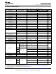
PACKAGE MATERIALS INFORMATION www.ti.com 5-Feb-2016 TAPE AND REEL INFORMATION *All dimensions are nominal Device Package Package Pins Type Drawing SPQ Reel Reel A0 Diameter Width (mm) (mm) W1 (mm) INA193AIDBVR SOT-23 DBV 5 3000 178.0 9.0 3.23 B0 (mm) K0 (mm) P1 (mm) W Pin1 (mm) Quadrant 3.17 1.37 4.0 8.0 Q3 INA193AIDBVT SOT-23 DBV 5 250 178.0 9.0 3.3 3.2 1.4 4.0 8.0 Q3 INA194AIDBVR SOT-23 DBV 5 3000 178.0 9.0 3.23 3.17 1.37 4.0 8.
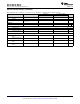
PACKAGE MATERIALS INFORMATION www.ti.com 5-Feb-2016 *All dimensions are nominal Device Package Type Package Drawing Pins SPQ Length (mm) Width (mm) Height (mm) INA193AIDBVR SOT-23 DBV 5 3000 180.0 180.0 18.0 INA193AIDBVT SOT-23 DBV 5 250 180.0 180.0 18.0 INA194AIDBVR SOT-23 DBV 5 3000 180.0 180.0 18.0 INA194AIDBVT SOT-23 DBV 5 250 180.0 180.0 18.0 INA195AIDBVR SOT-23 DBV 5 3000 180.0 180.0 18.0 INA195AIDBVT SOT-23 DBV 5 250 180.0 180.0 18.
IMPORTANT NOTICE Texas Instruments Incorporated and its subsidiaries (TI) reserve the right to make corrections, enhancements, improvements and other changes to its semiconductor products and services per JESD46, latest issue, and to discontinue any product or service per JESD48, latest issue. Buyers should obtain the latest relevant information before placing orders and should verify that such information is current and complete.