
Network Device User Guide


Device User Guide — 9S12C128DGV1/D V01.05
95
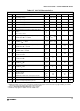
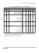
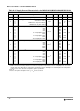
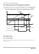
Appendix B Electrical Specifications
B.1 Voltage Regulator Operating Conditions
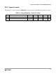
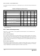
Table B-1 Voltage Regulator Electrical Parameters
Nu
m
C Characteristic Symbol Min Typical Max Unit
1 P Input Voltages
V
VDDR, A
2.97 — 5.5 V
2C
Regulator Current
Reduced Power Mode
Shutdown Mode
I
REG
—
—
20
12
50
40
µA
µA
3P
Output Voltage Core
Full Performance Mode
V
DD
2.35 2.5 2.75 V
4P
Low Voltage Interrupt
1
Assert Level C32, GC32
Assert Level C64, C96,C128
GC64, GC128
Deassert Level C32, GC32
Deassert Level C64, C96, C128
GC64, GC128
NOTES:
1. Monitors V
DDA
, active only in Full Performance Mode. Indicates I/O & ADC performance degradation due to low supply
voltage.
V
LVIA
V
LVIA
V
LVID
V
LVID
4.30
4.10
4.42
4.25
4.53
4.37
4.65
4.52
4.77
4.66
4.89
4.77
V
V
V
V
5P
Low Voltage Reset
2
Assert Level C32, GC32
Assert Level C64, C96, C128
GC64, GC128
2. Monitors V
DD
, active only in Full Performance Mode. MCU is monitored by the POR in RPM (see Figure B-1)
V
LVRA
2.25
2.25
2.3
2.35
—V
6P
Low Voltage Reset
(2)
Deassert Level
V
LVRD
——
2.55 V
7C
Power-on Reset
3
Assert Level
Deassert Level
3. Monitors V
DD
. Active in all modes.
NOTE:
The electrical characteristics given in this section are preliminary and should be
used as a guide only. Values in this section cannot be guaranteed by Motorola and
are subject to change without notice.
V
PORA
V
PORD
0.97
—
—
—
—
2.05
V
V