
Network Device User Guide


Device User Guide — 9S12C128DGV1/D V01.05
94
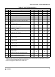
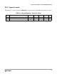
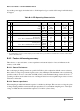
Table A-9 Supply Current Characteristics for MC9S12C64,MC9S12C96,MC9S12C128
Conditions are shown in Table A-4 with internal regulator enabled unless otherwise noted
Num C Rating Symbol Min Typ Max Unit
1 P Run Supply Current Single Chip,
I
DD5
45 mA
2
P
P
C
Wait Supply current
All modules enabled
VDDR<4.9V, only RTI enabled
(2)
VDDR>4.9V, only RTI enabled
I
DDW
2.5
3.5
33
8
mA
6
C
P
C
P
C
P
C
P
Pseudo Stop Current (RTI and COP disabled)
(2)(3)
-40°C
27°C
85°C
"C" Temp Option 100˚C
105°C
"V" Temp Option 120˚C
125°C
"M" Temp Option 140°C
I
DDPS
1
NOTES:
1. STOP current measured in production test at increased junction temperature, hence for Temp Option "C" the test is
carried out at 100˚C although the Temperature specification is 85˚C. Similarly for "v" and "M" options the temperature
used in test lies 15˚C above the temperature option specification.
190
200
300
400
450
600
650
1000
250
1400
1900
4800
µA
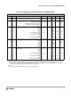
4
C
C
C
C
C
Pseudo Stop Current (RTI and COP enabled)
23
-40°C
27°C
85°C
105°C
125°C
2. PLL off
3. At those low power dissipation levels T
J
= T
A
can be assumed
I
DDPS
1
370
500
590
780
1200
µA
5
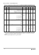
C
P
C
P
C
P
C
P
Stop Current
(3)
-40°C
27°C
85°C
"C" Temp Option 100˚C
105°C
"V" Temp Option 120˚C
125°C
"M" Temp Option 140°C
I
DDS
(1)
12
25
130
160
200
350
400
600
100
1200
1700
4500
µA