
Network Device User Guide


Device User Guide — 9S12C128DGV1/D V01.05
90
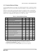
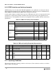
Table A-6 5V I/O Characteristics
Conditions are 4.5< VDDX <5.5V Termperature from -40˚C to +140˚C, unless otherwise noted
Num C Rating Symbol Min Typ Max Unit
1 P Input High Voltage
V
IH
0.65*V
DD5
--V
T Input High Voltage
V
IH
- - VDD5 + 0.3 V
2 P Input Low Voltage
V
IL
--
0.35*V
DD5
V
T Input Low Voltage
V
IL
VSS5 - 0.3 - - V
3 C Input Hysteresis
V
HYS
250 mV
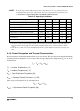
4P
Input Leakage Current (pins in high ohmic input
mode)
1
V
in
= V
DD5
or V
SS5
NOTES:
1. Maximum leakage current occurs at maximum operating temperature. Current decreases by approximately one-half for
each 8 C to 12 C in the temperature range from 50 C to 125 C.
I
in
–1 - 1 µA
5C
Output High Voltage (pins in output mode)
Partial Drive I
OH
= –2mA
V
OH
V
DD5
– 0.8
--V
6P
Output High Voltage (pins in output mode)
Full Drive IOH = –10mA
V
OH
V
DD5
– 0.8
--V
7C
Output Low Voltage (pins in output mode)
Partial Drive IOL = +2mA
V
OL
- - 0.8 V
8P
Output Low Voltage (pins in output mode)
Full Drive I
OL
= +10mA
V
OL
- - 0.8 V
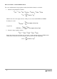
9P
Internal Pull Up Device Current,
tested at V
IL
Max.
I
PUL
- - -130 µA
10 C
Internal Pull Up Device Current,
tested at V
IH
Min.
I
PUH
-10 - - µA
11 P
Internal Pull Down Device Current,
tested at V
IH
Min.
I
PDH
- - 130 µA
12 C
Internal Pull Down Device Current,
tested at V
IL
Max.
I
PDL
10 - - µA
13 D Input Capacitance
C
in
7-pF
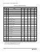
14 T
Injection current
2
Single Pin limit
Total Device Limit. Sum of all injected currents
2. Refer to Section A.1.4 Current Injection, for more details
I
ICS
I
ICP
-2.5
-25
- 2.5
25
mA
15 P
Port P, J Interrupt Input Pulse filtered
3
3. Parameter only applies in STOP or Pseudo STOP mode.
t
PIGN
3 µs
16 P
Port P, J Interrupt Input Pulse passed
3
t
PVAL
10 µs