
Network Device User Guide


Device User Guide — 9S12C128DGV1/D V01.05
89
Which is the sum of all output currents on I/O ports associated with VDDX and VDDR.
A.1.9 I/O Characteristics
This section describes the characteristics of all I/O pins. All parameters are not always applicable, e.g. not
all pins feature pull up/down resistances.
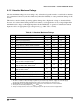
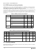
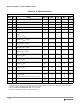
Table A-5 Thermal Package Characteristics
1
NOTES:
1. The values for thermal resistance are achieved by package simulations
Num C Rating Symbol Min Typ Max Unit
1T
Thermal Resistance LQFP48, single layer PCB
2
2. PC Board according to EIA/JEDEC Standard 51-2
θ
JA
--69
o
C/W
2T
Thermal Resistance LQFP48, double sided PCB with
2 internal planes
3
3. PC Board according to EIA/JEDEC Standard 51-7
θ
JA
--53
o
C/W
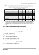
3 T Junction to Board LQFP48
θ
JB
30
o
C/W
4 T Junction to Case LQFP48
θ
JC
20
o
C/W
5 T Junction to Package Top LQFP48
Ψ
JT
4
o
C/W
6 T Thermal Resistance LQFP52, single sided PCB
θ
JA
--65
o
C/W
7T
Thermal Resistance LQFP52, double sided PCB with
2 internal planes
θ
JA
--49
o
C/W
8 T Junction to Board LQFP52
θ
JB
31
o
C/W
9 T Junction to Case LQFP52
θ
JC
17
o
C/W
10 T Junction to Package Top LQFP52
Ψ
JT
3
o
C/W
11 T Thermal Resistance QFP 80, single sided PCB
θ
JA
--52
o
C/W
12 T
Thermal Resistance QFP 80, double sided PCB with
2 internal planes
θ
JA
--42
o
C/W
13 T Junction to Board QFP80
θ
JB
28
o
C/W
14 T Junction to Case QFP80
θ
JC
18
o
C/W
15 T Junction to Package Top QFP80
Ψ
JT
4
o
C/W