
Network Device User Guide


Device User Guide — 9S12C128DGV1/D V01.05
88
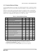
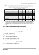
Two cases with internal voltage regulator enabled and disabled must be considered:
1. Internal Voltage Regulator disabled
Which is the sum of all output currents on I/O ports associated with VDDX and VDDM.
For R
DSON
is valid:
respectively
2. Internal voltage regulator enabled
I
DDR
is the current shown in Table A-8 and not the overall current flowing into VDDR, which
additionally contains the current flowing into the external loads with output high.
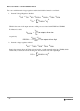
P
INT
I
DD
V
DD
⋅ I
DDPLL
V
DDPLL
⋅ I
DDA
+V
DDA
⋅+=
P
IO
R
DSON
i
∑
I
IO
i
2
⋅=
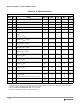
R
DSON
V
OL
I
OL
------------ for outputs driven low;=
R
DSON
V
DD5
V
OH
–
I
OH
------------------------------------ for outputs driven high;=
P
INT
I
DDR
V
DDR
⋅ I
DDA
V
DDA
⋅+=
P
IO
R
DSON
i
∑
I
IO
i
2
⋅=