
Network Device User Guide


Device User Guide — 9S12C128DGV1/D V01.05
66
latched into these bits on the rising edge of the reset signal. The ROMCTL signal allows the setting of the
ROMON bit in the MISC register thus controlling whether the internal Flash is visible in the memory map.
ROMON = 1 mean the Flash is visible in the memory map. The state of the ROMCTL pin is latched into
the ROMON bit in the MISC register on the rising edge of the reset signal.
For further explanation on the modes refer to the S12_MEBI block guide.
4.3 Security
The device will make available a security feature preventing the unauthorized read and write of the
memory contents. This feature allows:
• Protection of the contents of FLASH,
• Operation in single-chip mode,
• Operation from external memory with internal FLASH disabled.
The user must be reminded that part of the security must lie with the user’s code. An extreme example
would be user’s code that dumps the contents of the internal program. This code would defeat the purpose
of security. At the same time the user may also wish to put a back door in the user’s program. An example
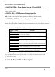
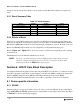
Table 4-1 Mode Selection
BKGD =
MODC
PE6 =
MODB
PE5 =
MODA
PP6 =
ROMCTL
ROMON
Bit
Mode Description
000X1
Special Single Chip, BDM allowed and ACTIVE. BDM is
allowed in all other modes but a serial command is
required to make BDM active.
001
01
Emulation Expanded Narrow, BDM allowed
10
0 1 0 X 0 Special Test (Expanded Wide), BDM allowed
011
01
Emulation Expanded Wide, BDM allowed
10
1 0 0 X 1 Normal Single Chip, BDM allowed
101
00
Normal Expanded Narrow, BDM allowed
11
110X1
Peripheral; BDM allowed but bus operations would cause
bus conflicts (must not be used)
111
00
Normal Expanded Wide, BDM allowed
11
Table 4-2 Clock Selection Based on PE7
PE7 = XCLKS Description
1 Colpitts Oscillator selected
0 Pierce Oscillator/external clock selected