
Network Device User Guide


Device User Guide — 9S12C128DGV1/D V01.05
56
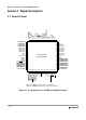
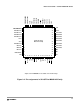
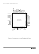
2.2.1 Pin Initialization for 48 & 52 Pin LQFP bond-out versions
Not Bonded Pins If the port pins are not bonded out in the chosen package the user should initialize the
registers to be inputs with enabled pull resistance to avoid excess current consumption. This applies to the
following pins:
(48LQFP): Port A[7:1], Port B[7:5], Port B[3:0], PortE[6,5,3,2], Port P[7:6], PortP[4:0], Port J[7:6],
PortS[3:2]
(52LQFP): Port A[7:3], Port B[7:5], Port B[3:0], PortE[6,5,3,2], Port P[7:6], PortP[2:0], Port J[7:6],
PortS[3:2]
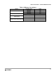
PP[2:0] KWP[2:0] PW[2:0] VDDX
PERP/
PPSP
Disabled Port P I/O Pins, keypad wake-up, PWM outputs
PJ[7:6] KWJ[7:6] — VDDX
PERJ/
PPSJ
Disabled Port J I/O Pins and keypad wake-up
PM5 SCK — VDDX
PERM/
PPSM
Up Port M I/O Pin and SPI SCK signal
PM4
MOSI
— VDDX
PERM/
PPSM
Up Port M I/O Pin and SPI
MOSI
signal
PM3
SS — VDDX
PERM/
PPSM
Up Port M I/O Pin and SPI SS signal
PM2
MISO
— VDDX
PERM/
PPSM
Up Port M I/O Pin and SPI
MISO
signal
PM1 TXCAN — VDDX
PERM/
PPSM
Up
Port M I/O Pin and CAN transmit signal
2
PM0 RXCAN — VDDX
PERM/
PPSM
Up
Port M I/O Pin and CAN receive signal
2
PS[3:2] — — VDDX
PERS/
PPSS
Up Port S I/O Pins
PS1 TXD — VDDX
PERS/
PPSS
Up Port S I/O Pin and SCI transmit signal
PS0 RXD — VDDX
PERS/
PPSS
Up Port S I/O Pin and SCI receive signal
PT[7:5] IOC[7:5] — VDDX
PERT/
PPST
Disabled Port T I/O Pins shared with timer (TIM)
PT[4:0] IOC[4:0] PW[4:0] VDDX
PERT/
PPST
Disabled Port T I/O Pins shared with timer and PWM
NOTES:
1. The PortE output buffer enable signal control at reset is determined by the PEAR register and is mode dependent. E.g. in
special test mode RDWE=LSTRE=1 which enables the PE[3:2] output buffers and disables the pull-ups. Refer to S12_MEBI
user guide for PEAR register details.
2. CAN functionality is not available on the MC9S12GC-Family members
Pin Name
Function 1
Pin Name
Function 2
Pin Name
Function 3
Power
Domain
Internal Pull
Resistor
Description
CTRL
Reset
State