
Network Device User Guide

Device User Guide — 9S12C128DGV1/D V01.05
50
1.7 Part ID Assignments
The part ID is located in two 8-bit registers PARTIDH and PARTIDL (addresses $001A and $001B after
reset). The read-only value is a unique part ID for each revision of the chip. Table 1-3 shows the assigned
part ID numbers.
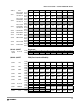
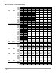
The device memory sizes are located in two 8-bit registers MEMSIZ0 and MEMSIZ1 (addresses $001C
and $001D after reset). Table 1-4 shows the read-only values of these registers. Refer to Module Mapping
and Control (MMC) Block Guide for further details.
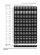
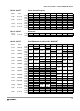
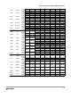
$0280 - $03FF Reserved space
Address Name Bit 7 Bit 6 Bit 5 Bit 4 Bit 3 Bit 2 Bit 1 Bit 0
$0280
- $2FF
Reserved
Read: 00000000
Write:
$0300 -
$03FF
Unimplemented
Read: 00000000
Write:
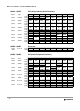
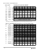
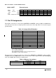
Table 1-3 Assigned Part ID Numbers
Device Mask Set Number
Part ID
1
NOTES:
1. The coding is as follows:
Bit 15-12: Major family identifier
Bit 11-8: Minor family identifier
Bit 7-4: Major mask set revision number including FAB transfers
Bit 3-0: Minor - non full - mask set revision
MC9S12C32 0L45J $3300
MC9S12C32 1L45J $3300
MC9S12C32 2L45J $3302
MC9S12C64 TBD TBD
MC9S12C96 TBD TBD
MC9S12C128 0L09S $3100
MC9S12C128 1L09S $3101
MC9S12GC16 TBD TBD
MC9S12GC32 TBD TBD
MC9S12GC64 TBD TBD
MC9S12GC128 TBD TBD
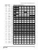
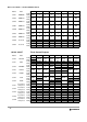
Table 1-4 Memory size registers
Device Register name Value
MC9S12GC16
MEMSIZ0 $00
MEMSIZ1 $80