
Network Device User Guide

Device User Guide — 9S12C128DGV1/D V01.05
44
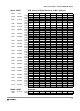
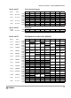
$00F7 PWMPER5
Read:
Bit 7 6 5 4 3 2 1 Bit 0
Write:
$00F8 PWMDTY0
Read:
Bit 7 6 5 4 3 2 1 Bit 0
Write:
$00F9 PWMDTY1
Read:
Bit 7 6 5 4 3 2 1 Bit 0
Write:
$00FA PWMDTY2
Read:
Bit 7 6 5 4 3 2 1 Bit 0
Write:
$00FB PWMDTY3
Read:
Bit 7 6 5 4 3 2 1 Bit 0
Write:
$00FC PWMDTY4
Read:
Bit 7 6 5 4 3 2 1 Bit 0
Write:
$00FD PWMDTY5
Read:
Bit 7 6 5 4 3 2 1 Bit 0
Write:
$00FE Reserved
Read: 00000000
Write:
$00FF Reserved
Read: 00000000
Write:
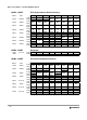
$0100 - $010F Flash Control Register
Address Name Bit 7 Bit 6 Bit 5 Bit 4 Bit 3 Bit 2 Bit 1 Bit 0
$0100 FCLKDIV
Read: FDIVLD
PRDIV8 FDIV5 FDIV4 FDIV3 FDIV2 FDIV1 FDIV0
Write:
$0101 FSEC
Read: KEYEN1 KEYEN0 NV5 NV4 NV3 NV2 SEC1 SEC0
Write:
$0102 FTSTMOD
Read:
0 0 0 WRALL
000
0
Write:
$0103 FCNFG
Read:
CBEIE CCIE KEYACC
000
BKSEL1 BKSEL0
Write:
$0104 FPROT
Read:
FPOPEN NV6 FPHDIS FPHS1 FPHS0 FPLDIS FPLS1 FPLS0
Write:
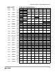
$0105
FSTAT
Read:
CBEIF
CCIF
PVIOL ACCERR
0
BLANK
00
Write:
$0106 FCMD
Read: 0
CMDB6 CMDB5
00
CMDB2
0
CMDB0
Write:
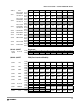
$0107
Reserved for
Factory Test
Read: 00000000
Write:
$0108
Reserved for
Factory Test
Read: 00000000
Write:
$0109
Reserved for
Factory Test
Read: 00000000
Write:
$010A
Reserved for
Factory Test
Read: 00000000
Write:
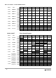
$010B
Reserved for
Factory Test
Read: 00000000
Write:
Address Name Bit 7 Bit 6 Bit 5 Bit 4 Bit 3 Bit 2 Bit 1 Bit 0