
Network Device User Guide


Device User Guide — 9S12C128DGV1/D V01.05
35
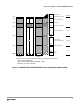
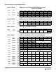
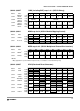
$0018 - $0018 Miscellaneous Peripherals (Device User Guide)
$0019 - $0019 VREG3V3 (Voltage Regulator)
$0012 INITEE
Read:
EE15 EE14 EE13 EE12 EE11
00
EEON
Write:
$0013 MISC
Read: 0000
EXSTR1 EXSTR0 ROMHM ROMON
Write:
$0014 Reserved
Read: 00000000
Write:
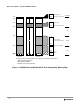
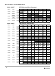
$0015 - $0016 INT map 1 of 2 (HCS12 Interrupt)
Address Name Bit 7 Bit 6 Bit 5 Bit 4 Bit 3 Bit 2 Bit 1 Bit 0
$0015 ITCR
Read: 0 0 0
WRINT ADR3 ADR2 ADR1 ADR0
Write:
$0016 ITEST
Read:
INTE INTC INTA INT8 INT6 INT4 INT2 INT0
Write:
$0017 - $0017 MMC map 2 of 4 (HCS12 Module Mapping Control)
Address Name Bit 7 Bit 6 Bit 5 Bit 4 Bit 3 Bit 2 Bit 1 Bit 0
$0017 Reserved
Read: 00000000
Write:
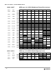
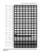
Address Name Bit 7 Bit 6 Bit 5 Bit 4 Bit 3 Bit 2 Bit 1 Bit 0
$0018 Reserved
Read: 00000000
Write:
Address Name Bit 7 Bit 6 Bit 5 Bit 4 Bit 3 Bit 2 Bit 1 Bit 0
$0019 VREGCTRL
Read: 00000LVDS
LVIE LVIF
Write:
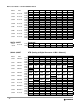
$001A - $001B Miscellaneous Peripherals (Device User Guide)
Address Name Bit 7 Bit 6 Bit 5 Bit 4 Bit 3 Bit 2 Bit 1 Bit 0
$001A PARTIDH
Read: ID15 ID14 ID13 ID12 ID11 ID10 ID9 ID8
Write:
$001B PARTIDL
Read: ID7 ID6 ID5 ID4 ID3 ID2 ID1 ID0
Write:
$0010 - $0014 MMC map 1 of 4 (HCS12 Module Mapping Control)
Address Name Bit 7 Bit 6 Bit 5 Bit 4 Bit 3 Bit 2 Bit 1 Bit 0