
Network Device User Guide

Device User Guide — 9S12C128DGV1/D V01.05
28
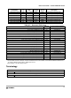
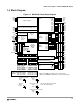
1.5 Device Memory Map
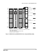
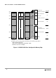
Table 1-1 shows the device register map of the MC9S12C-Family after reset. The following figures
(Figure 1-2, Figure 1-2, Figure 1-3 and Figure 1-4) illustrate the full device memory map with flash
and RAM.
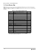
Table 1-1 Device Register Map Overview
Address Module Size
$000 - $017 CORE (Ports A, B, E, Modes, Inits, Test) 24
$018 Reserved 1
$019 Voltage Regulator (VREG) 1
$01A - $01B Device ID register 2
$01C - $01F CORE (MEMSIZ, IRQ, HPRIO) 4
$020 - $02F CORE (DBG) 16
$030 - $033
CORE (PPAGE
1
)
NOTES:
1. External memory paging is not supported on this device (6.1.1 PPAGE).
4
$034 - $03F Clock and Reset Generator (CRG) 12
$040 - $06F Standard Timer Module16-bit 8-channels (TIM) 48
$070 - $07F Reserved 16
$080 - $09F Analog to Digital Convert (ATD) 32
$0A0 - $0C7 Reserved 40
$0C8 - $0CF Serial Communications Interface (SCI) 8
$0D0 - $0D7 Reserved 8
$0D8 - $0DF Serial Peripheral Interface (SPI) 8
$0E0 - $0FF Pulse Width Modulator 8-bit 6 channels (PWM) 32
$100 - $10F Flash Control Register 16
$110 - $13F Reserved 48
$140 - $17F
Motorola Scalable CAN (MSCAN)
2
2. Not available on MC9S12GC-Family Devices
64
$180 - $23F Reserved 192
$240 - $27F Port Integration Module (PIM) 64
$280 - $3FF Reserved 384