
Network Device User Guide
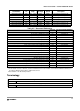


Device User Guide — 9S12C128DGV1/D V01.05
25
– Pierce or low current Colpitts oscillator
– Phase-locked loop clock frequency multiplier
– Limp home mode in absence of external clock
– Low power 0.5 to 16 MHz crystal oscillator reference clock
• Operating frequency
– 32MHz equivalent to 16MHz Bus Speed for single chip
– 32MHz equivalent to 16MHz Bus Speed in expanded bus modes
– Option of 9S12C-Family: 50MHz equivalent to 25MHz Bus Speed
– All 9S12GC-Family Members allow a 50MHz operting frequency.
• Internal 2.5V Regulator
– Supports an input voltage range from 2.97V to 5.5V
– Low power mode capability
– Includes low voltage reset (LVR) circuitry
– Includes low voltage interrupt (LVI) circuitry
• 48-Pin LQFP, 52-Pin LQFP or 80-Pin QFP package
– Up to 58 I/O lines with 5V input and drive capability (80 pin package)
– Up to 2 dedicated 5V input only lines (IRQ, XIRQ)
– 5V 8 A/D converter inputs and 5V I/O
• Development support
– Single-wire background debug™ mode (BDM)
– On-chip hardware breakpoints
– Enhanced DBG12 debug features
1.3 Modes of Operation
User modes (Expanded modes are only available in the 80 pin package version).
• Normal and Emulation Operating Modes
– Normal Single-Chip Mode
– Normal Expanded Wide Mode
– Normal Expanded Narrow Mode
– Emulation Expanded Wide Mode
– Emulation Expanded Narrow Mode
• Special Operating Modes